

Deep hole silicon etching method
A deep-hole silicon etching, etching gas technology, applied in decorative arts, gaseous chemical plating, microstructure technology, etc., can solve the problems of reduced through-hole sidewall smoothness, reduced etching efficiency, etc., to achieve good smoothness The effect of reducing the switching time and improving the etching efficiency
- Summary
- Abstract
- Description
- Claims
- Application Information
AI Technical Summary
Problems solved by technology
Method used
Image

Examples
Embodiment Construction
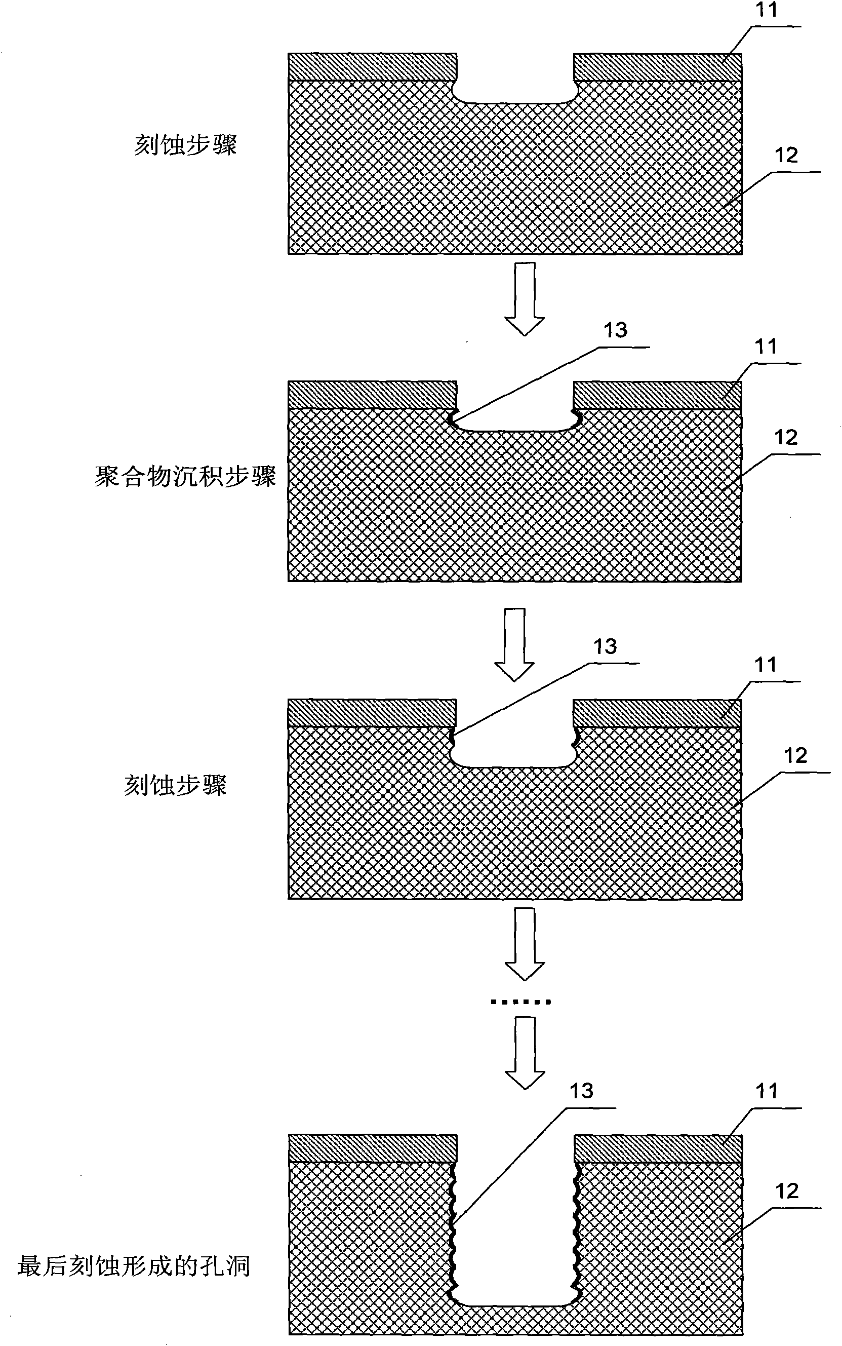
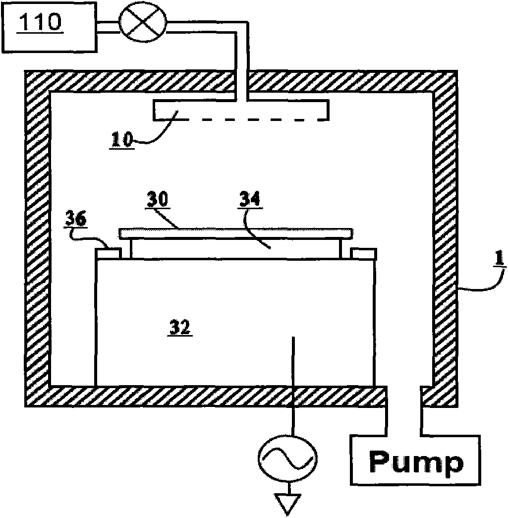
[0013] In order to make the object, technical solution and advantages of the present invention clearer, the present invention will be further described in detail below in conjunction with the accompanying drawings. figure 2 Shown is the structural diagram of the reaction chamber for plasma etching used in the present invention. The plasma reaction chamber comprises a chamber body 1, which includes a pedestal and a lower electrode 32 for placing a processed substrate in the chamber. Above the lower electrode 32 is a device 34 for fixing the substrate to be processed, which can be an electrostatic chuck (ESC ). On the electrostatic chuck is a substrate 30 to be processed, and the periphery of the substrate 30 also includes an edge ring 36 for adjusting the electric field and temperature distribution at the edge of the substrate. The top of the reaction chamber corresponding to the substrate 30 to be processed includes a gas distribution device 10, such as a gas shower head. T...
PUM
| Property | Measurement | Unit |
|---|---|---|
| Opening depth | aaaaa | aaaaa |
Abstract
Description
Claims
Application Information