
Method for manufacturing vertical LED chip

An LED chip, vertical structure technology, applied in the field of optoelectronic information, can solve the problems of mechanical damage, poor controllability of mechanical stress grinding thickness, damage to the N-type gallium nitride layer, etc., to avoid selectivity, improve chip yield and thickness Highly controllable effect

Active Publication Date: 2014-08-27
HANGZHOU SILAN AZURE
View PDF5 Cites 0 Cited by
  • Summary
  • Abstract
  • Description
  • Claims
  • Application Information

AI Technical Summary

Problems solved by technology

However, in the method of removing the sapphire substrate through preliminary rough grinding and mechanical grinding, due to the mechanical stress of the preliminary rough grinding and mechanical grinding and the poor controllability of the grinding thickness, the buffer layer will be ground and removed during the grinding process, and even damage the underlying substrate. N-type GaN layer, causing severe mechanical damage

Method used


Image

  • Method for manufacturing vertical LED chip
  • Method for manufacturing vertical LED chip
  • Method for manufacturing vertical LED chip

Examples


Embodiment Construction

[0029] In order to make the content of the present invention clearer and easier to understand, the content of the present invention will be further described below in conjunction with the accompanying drawings. Of course, the present invention is not limited to this specific embodiment, and general replacements known to those skilled in the art are also covered within the protection scope of the present invention.

[0030] Secondly, the present invention is described in detail by means of schematic diagrams. When describing the examples of the present invention in detail, for the convenience of explanation, the schematic diagrams are not partially enlarged according to the general scale, which should not be used as a limitation of the present invention.

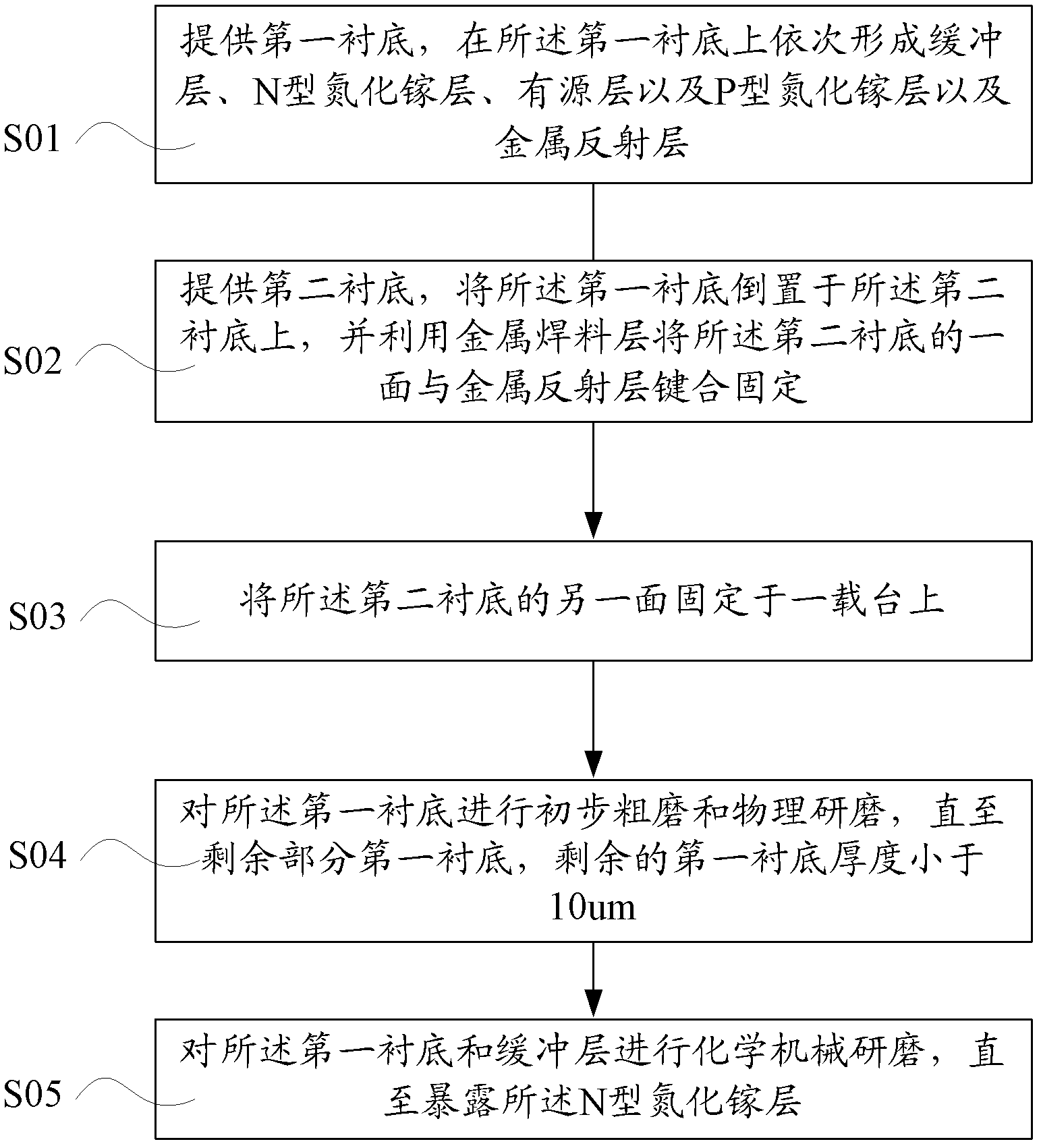
[0031] Such as figure 1 Shown, it is the manufacturing method of vertical structure LED chip described in one embodiment of the present invention, comprises the following steps:

[0032] Step S01: providing a first substrate...


PUM

PropertyMeasurementUnit
diameteraaaaaaaaaa
wavelengthaaaaaaaaaa
thicknessaaaaaaaaaa

Abstract

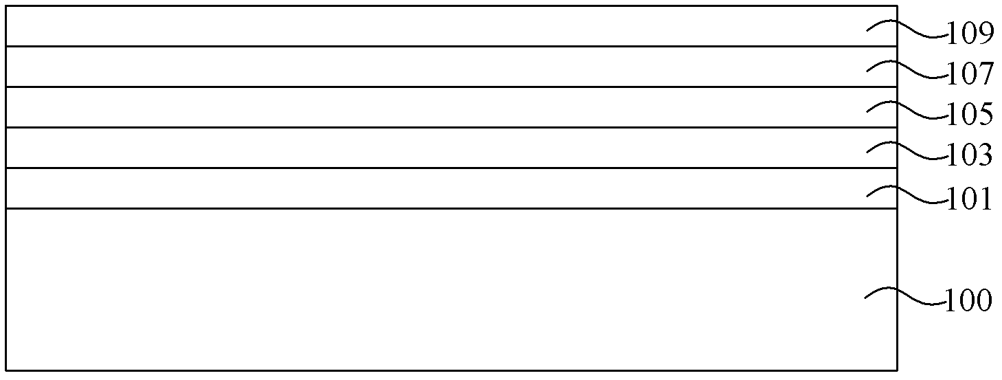
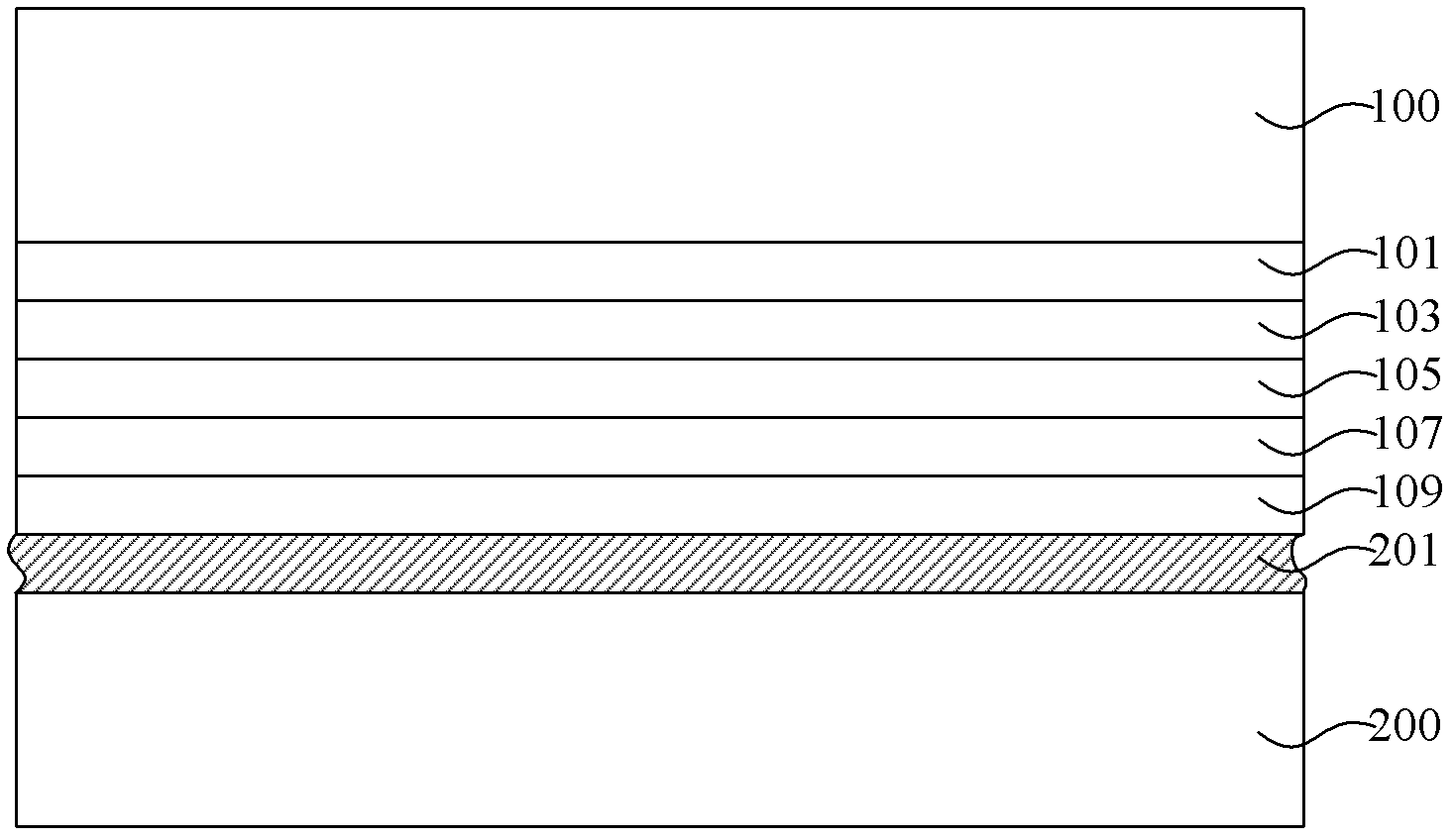
The invention relates to a method for manufacturing a vertical LED chip, which comprises the following steps of: providing a first substrate, and forming in sequence a buffer layer, an N type gallium nitride layer, an active layer and a P type gallium nitride layer as well as a metal reflection layer on the first substrate; providing a second substrate, inverting the first substrate on the second one, and using a metal welding material layer to fixedly bond one surface of the second substrate with the metal reflection layer; fixing the other surface of the second substrate to a carrying table; initially roughly grinding and physically grinding the first substrate and the buffer layer until part of the first substrate is remained, wherein the thickness of the remained first substrate is less than 10um; and chemically and mechanically grinding the first substrate until the N type gallium nitride layer is exposed. The production efficiency and yield of the vertical LED chip in a process of stripping off the substrate can be improved by the method.

Description

technical field [0001] The invention relates to the field of optoelectronic information technology, in particular to a substrate peeling method for a vertical structure LED chip substrate. Background technique [0002] In the manufacturing process of LED chips, the heterogeneous epitaxy technology of forming a gallium nitride layer on a sapphire substrate is a cash-mature epitaxy technology, but the sapphire substrate is a non-conductive substrate, which hinders the development of high-power and high-current chips. [0003] In nitride-based semiconductor devices, sapphire is often used as a substrate. Since sapphire is an insulator, it is also difficult to open holes on its surface. When using sapphire as the substrate, the two electrodes of the light-emitting element grown on the sapphire must be on the same side, so that not only the effective light-emitting area will be reduced, but also there are two electrodes on the same surface, and the local current density will be ...

Claims


Application Information

Patent Timeline
Patent Type & Authority Patents(China)
IPC IPC(8): H01L33/44H01L33/12H01L33/00
Inventor 张昊翔金豫浙江忠永
Owner HANGZHOU SILAN AZURE
Learn More