
Mask and method of making the same

A mask, conductive mask technology, used in semiconductor/solid-state device manufacturing, vacuum evaporation plating, coating, etc., can solve the problems of large pattern error and low accuracy, and achieve small pattern error and high accuracy. Effect

Active Publication Date: 2021-01-26
BOE TECH GRP CO LTD +1
View PDF12 Cites 0 Cited by
  • Summary
  • Abstract
  • Description
  • Claims
  • Application Information

AI Technical Summary

Problems solved by technology

[0003] The present application provides a mask and its manufacturing method, which can solve the problem of large error and low precision of patterns formed by vapor deposition using a mask

Method used


Image

  • Mask and method of making the same
  • Mask and method of making the same
  • Mask and method of making the same

Examples


Embodiment Construction

[0038] In order to make the purpose, technical solution and advantages of the present application clearer, the implementation manners of the present application will be further described in detail below in conjunction with the accompanying drawings.

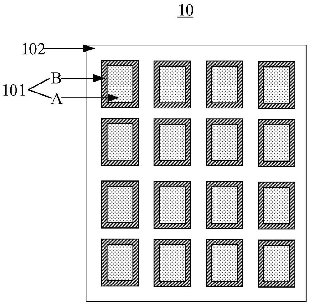
[0039] figure 1 It is a structural schematic diagram of a display motherboard known to the inventor, such as figure 1 As shown, the display motherboard 10 includes a plurality of display screens 101 formed on a base substrate 102 . Each display screen 101 includes a display area A and a non-display area B around the display area A. In the preparation obtained as figure 1 After the display screen motherboard 10 is shown, multiple display screens 101 are obtained by cutting the display screen motherboard 10 .

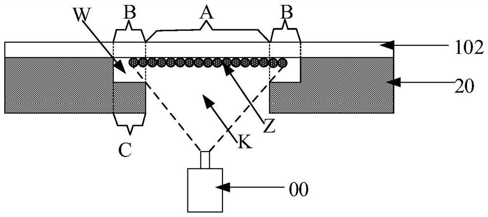
[0040] In the related art, a mask plate is usually used to form the entire layer structure in the display screen through an evaporation process. figure 2 It is a schematic diagram of a scene where a mask is used to form...


PUM

PropertyMeasurementUnit
thicknessaaaaaaaaaa

Abstract

The application discloses a mask plate and a manufacturing method thereof, which belong to the field of display technology. The mask plate is used to prepare a display screen motherboard through an evaporation process. The display screen motherboard includes a display screen, and the display screen has a display area and a non-display area located around the display area. The mask plate includes: a conductive mask substrate, and the metal film layer on one side of the conductive mask substrate, the conductive mask substrate is provided with an opening, the size and shape of the opening are equal to the size and shape of the display area; the conductive mask substrate has a first area and a second area, the second A region surrounds and is adjacent to the opening, the size of the first region is greater than or equal to the size of the non-display region, and the orthographic projection of the metal film layer on the conductive mask substrate coincides with the second region. The present application solves the problem that the patterns formed by vapor deposition using a mask plate have large errors and low precision. This application is used to prepare display motherboards.

Description

technical field [0001] The present application relates to the field of display technology, in particular to a mask and a manufacturing method thereof. Background technique [0002] In the preparation process of an organic light-emitting diode (Organic Light-Emitting Diode, OLED) display screen, usually firstly, a display board is manufactured on a base substrate, and the display board includes a plurality of display screens arranged in an array, Then cut the motherboard of the display screen to obtain the display screen. Wherein, the whole-layer structure in the display screen can be formed through an evaporation process using a mask, and the whole-layer structure includes an electron transport layer, a hole transport layer, and a cathode layer. Contents of the invention [0003] The present application provides a mask plate and a manufacturing method thereof, which can solve the problem of large error and low precision of patterns formed by vapor deposition using a mask ...

Claims


Application Information

Patent Timeline
Patent Type & Authority Patents(China)
IPC IPC(8): C23C14/04C23C14/12C23C14/24C25D5/02C25D7/00H01L51/56
CPCC23C14/04C23C14/12C23C14/24C25D5/02C25D7/00H10K71/00H10K71/166
Inventor 张微
Owner BOE TECH GRP CO LTD
Learn More