Laser bonding method for packaging of photoelectric device

A photoelectric device and bonding technology, which is applied in the field of laser bonding, can solve the problems of incomplete protection of the glass sealing body, high price, cracks in the glass substrate, etc.

Active Publication Date: 2012-04-04
SHANGHAI UNIV
View PDF3 Cites 29 Cited by
  • Summary
  • Abstract
  • Description
  • Claims
  • Application Information

AI Technical Summary

Problems solved by technology

Although epoxy resin encapsulation can provide effective mechanical strength, it is expensive and limits its use, and it cannot completely protect the glass seal
Metal bonding cannot be used for a long time in a large temperature range due to the large difference in CTE between metal and glass
At present, the method of laser bonding glass sealing material is applied to the sealing body

Method used


Image

  • Laser bonding method for packaging of photoelectric device
  • Laser bonding method for packaging of photoelectric device
  • Laser bonding method for packaging of photoelectric device

Examples


Embodiment Construction

[0024] With reference to the accompanying drawings, the preferred embodiments of the present invention are described in detail as follows.

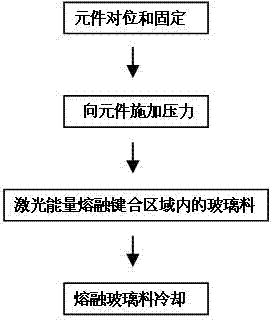
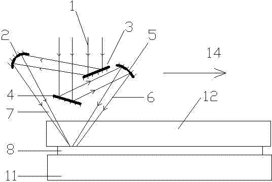
[0025] Examples see Figure 1 ~ Figure 3 , the laser bonding method that the present invention is used for optoelectronic device packaging comprises the following steps:

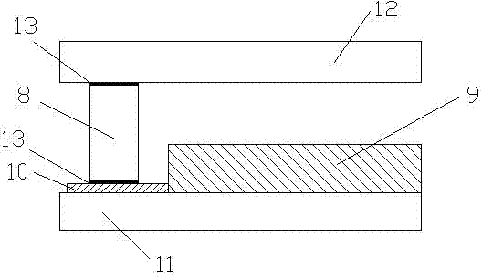
[0026] a. The glass cover plate 12 pre-sintered with the glass sealant and the glass substrate 11 deposited with the optoelectronic device 9 are accurately aligned and fixed by a fixture; the glass sealant is deposited on the edge of the glass cover plate 11 by screen printing Inside, and constitute the glass seal 8, the glass cover plate 12 and the glass substrate 11 respectively form a bonding surface area 13 in direct contact with the glass seal 8 under the action of laser energy; the optoelectronic device 9 is located inside the glass seal 8;

[0027] b. Apply initial pressure to the glass cover plate 12 and the glass substrate 11 in step a, so that the glass cover...


PUM


Abstract

The invention discloses a laser bonding method for packaging of a photoelectric device, which comprises the following steps of: accurately positioning and fixing elements to be welded; applying an initial clamping force to the elements to be welded to tightly bond the elements to be welded with glass sealing materials; and in the bonding process, moving and heating the glass materials by using double beam laser obtained by light splitting method, preheating the glass sealing materials by the previous laser, melting the glass sealing materials by the next laser, forming a sealing body on a glass substrate plane, and providing airtight sealing. The laser bonding method provided by the invention remarkably reduces a residual stress distribution state of the cooled glass and has an outstanding effect for improving the packaging quality and prolonging the service life of the photoelectric device. Some examples of such glass packaging body are an organic light-emitting diode (OLED) display and other optical devices. The OLED device is taken as an example for presentation in the laser bonding method.

Description

technical field [0001] The invention relates to a laser bonding method for photoelectric device packaging, which is suitable for the packaging of organic light-emitting diode (OLED) displays, solar cells and other photoelectric devices, and belongs to the technical field of photoelectric device packaging technology and equipment. Background technique [0002] Traditional OLED device encapsulation techniques include: epoxy resin encapsulation and metal bonding using inorganic fillers and / or organic fillers. Although epoxy resin encapsulation can provide effective mechanical strength, its high price limits its use, and it cannot completely protect the glass sealing body. Metal bonding cannot be used for a long time in a large temperature range due to the large difference in CTE between metal and glass. At present, the method of laser bonding glass sealing material is applied to the sealing body of OLED devices. Since the laser beam is used to move and heat the glass sealing m...

Claims


Application Information

Patent Timeline
IPC IPC(8): H01L51/56
Inventor 张建华赖禹能陈遵淼李懋瑜黄元昊
Owner SHANGHAI UNIV
Why Eureka
Try Eureka