

Exposure method adopting lithography machine
An exposure method and technology of lithography machine, applied in the field of lithography machine exposure, can solve problems such as chip deformation, and achieve the effect of the best process registration progress
- Summary
- Abstract
- Description
- Claims
- Application Information
AI Technical Summary
Problems solved by technology
Method used
Image

Examples
Embodiment Construction
[0026] Embodiments of the present invention will be described in detail below. It should be noted that the embodiments described here are for illustration only, and are not intended to limit the present invention.
[0027] Figure 4 Exemplary shows the flow chart of the exposure method of the lithography machine of the present invention, including
[0028] Step 101, transfer the silicon wafer to the silicon wafer loading stage.
[0029] Step 102, turn on the vacuum equipment to make the silicon wafer carrier absorb the silicon wafer.
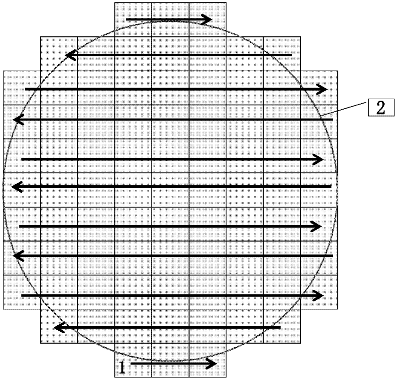
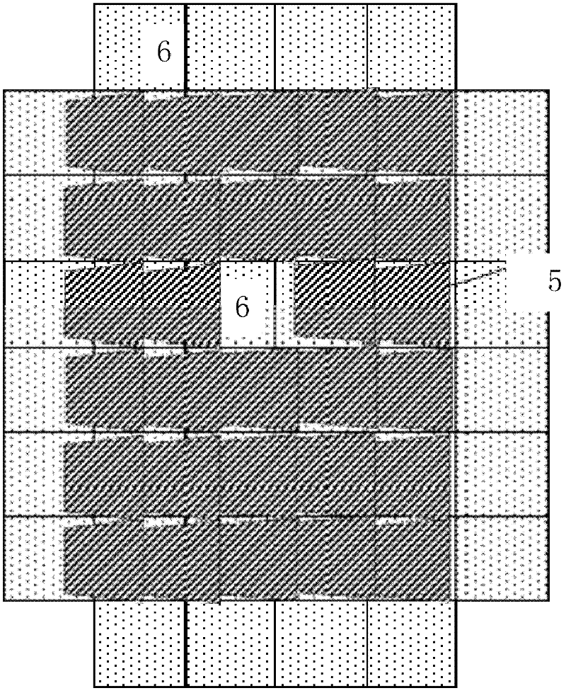
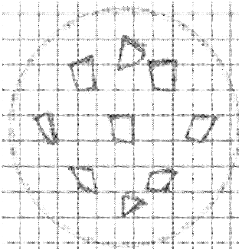
[0030] Step 103 , perform alignment, and expose the chips on the silicon wafer in batches, wherein the chips are exposed at intervals on the exposure path during each batch of exposure.
[0031] The implementation process of the exposure method for the lithography machine of the present invention will be described in detail below.
[0032] If the traditional continuous exposure method is adopted, the exposed chip will be deformed due to high...
PUM
 Abstract
Description
Claims
Application Information