Cut/ground silicon wafer surface cleaning method

A silicon wafer surface and silicon wafer technology, which is applied in the field of cutting and grinding silicon wafer surface cleaning, can solve the problems of shortening the normal service cycle of the cleaning solution, poor repeatability of the surface cleanliness of the cleaned silicon wafer, and poor ultrasonic cavitation effect, etc. To achieve the effect of improved cleaning quality and economic benefits, lasting and effective decontamination ability, and improved effective service cycle

Inactive Publication Date: 2012-04-11
沈利军
View PDF5 Cites 30 Cited by
  • Summary
  • Abstract
  • Description
  • Claims
  • Application Information

AI Technical Summary

Problems solved by technology

[0004] In mass production, the silicon wafers are cleaned by the process method in the above table. When the products are supplied to the device factory for use, it often occurs that when the texture is made on the surface of the silicon wafer, the color of the textured layer is inconsistent, which seriously affects the conversion efficiency of solar cells; There are TRR contamination phenomena in the manufacture of silicon rectifier diodes and other devices, resulting in low reverse recovery time, and the problem of scrapping because the parameters do not meet the design and use requirements; When the silicon substrate is diffused, there will be adhesion and cake formation between the chips, resulting in broken chips and scrapped problems
[0005] Analysis of the reasons for the above-mentioned problems in the use of the existing cleaning technology is mainly: the cleaning process is unreasonably set up, the silicon wafers after the two-station acid bubbling ultrasonic cleaning, together with the flower basket and the basket carrying the silicon wafer flower basket, After being directly transferred to the three-station alkaline cleaning liquid ultrasonic cleaning tank for super-washing, it is then transferred to the four-station alkaline cleaning liquid ultrasonic cleaning tank for super-washin

Method used


Image

  • Cut/ground silicon wafer surface cleaning method
  • Cut/ground silicon wafer surface cleaning method
  • Cut/ground silicon wafer surface cleaning method

Examples


Embodiment Construction

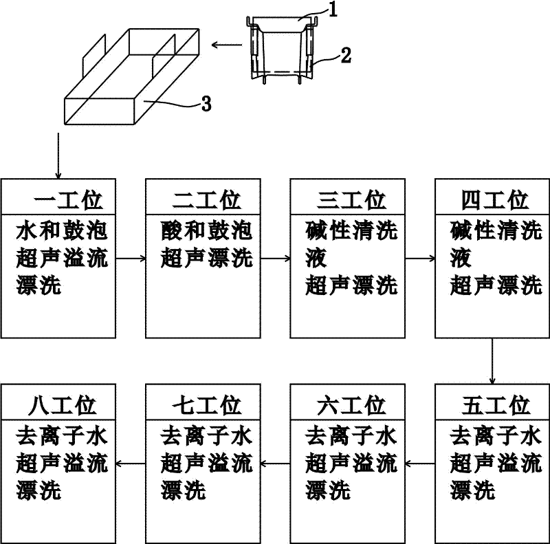
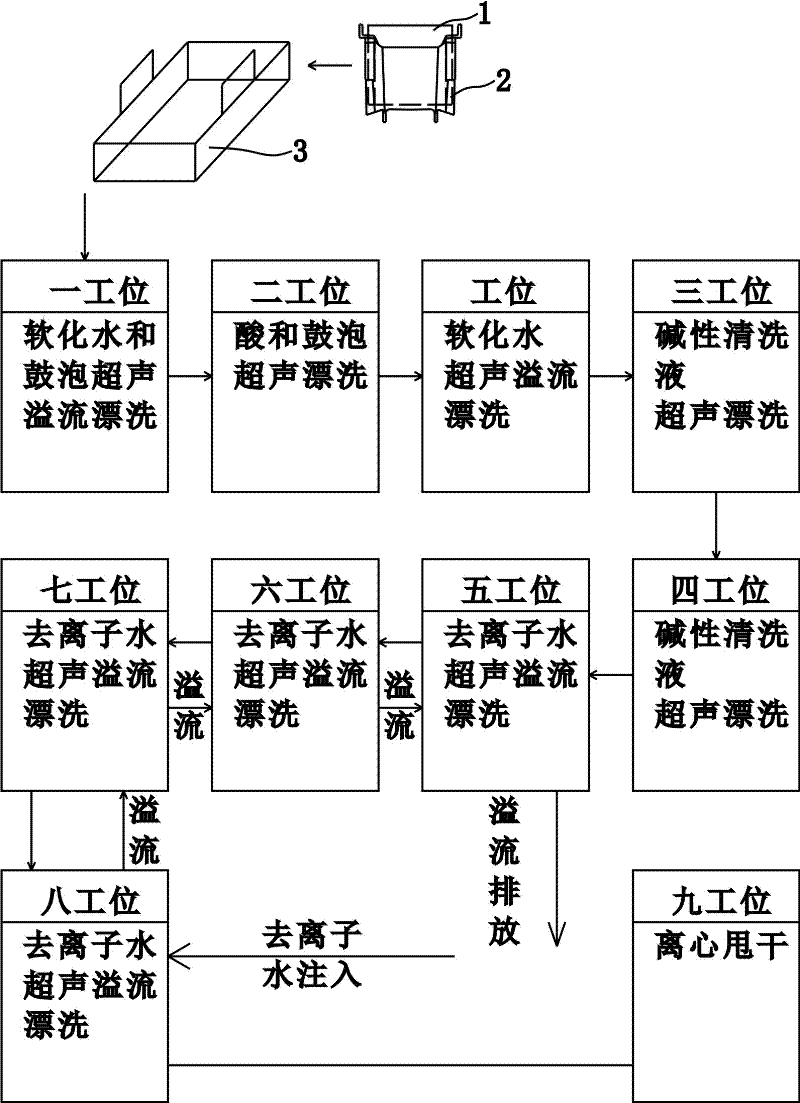
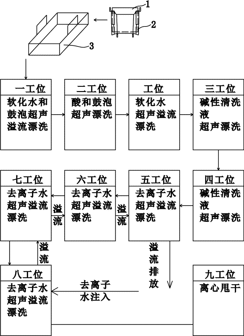
[0022] see figure 2 , this implementation case includes the silicon chip 1, the carrier of the silicon chip 1, that is, the carrying basket 2 and the basket 3 carrying the flower basket, and the silicon chip 1 and the carrier are immersed in sequence,

[0023] Ultrasonic overflow rinsing in a cleaning tank with demineralized water and bubbling;

[0024] Ultrasonic cleaning in the cleaning tank with 3~5% HF acid solution and bubbling two stations;

[0025] Ultrasonic overflow rinsing in the cleaning tank with softened water station;

[0026] Ultrasonic cleaning in the three-station cleaning tank with alkaline cleaning agent;

[0027] Ultrasonic cleaning of four-station cleaning tank with alkaline cleaning agent;

[0028] Ultrasonic overflow rinsing in five to eight station cleaning tanks equipped with high-purity deionized water,

[0029] The silicon wafer 1 together with the carrier is washed with deionized water at eight stations, and then enters a nine-station centrifug...


PUM


Abstract

The invention discloses a cut/ground silicon wafer surface cleaning method. A silicon wafer and a silicon wafer carrier are sequentially immersed into the following stations and cleaned in corresponding processes: ultrasonic overflow rinsing in a first station cleaning tank with softened water and bubbles and the like. The cut/ground silicon wafer surface cleaning method overcomes the problem of easy acid-alkali neutralization reaction, so that the PH value and concentration of the alkaline cleaner of a third station and a fourth station can be kept constant, and thereby the dirt-removing capability of the alkaline cleaner can be persistently effective. The cut/ground silicon wafers cleaned by the method have high surface cleanliness, good repeatability and a consistent color; the oxidation phenomena of mottling, bluing and blacking are prevented, and the acceptance rate of the cleaned silicon wafers is high; meanwhile, the cleaner does not need to be added in the effective period of cleaning capacity specified by the process, the cut/ground silicon wafer surface cleaning method is easy to operate, however, the effective service period of the cleaner is doubled, and the cleaning cost is greatly reduced; and the cleaning quality and the economic benefit are remarkably increased.

Description

technical field [0001] The invention relates to a method for cleaning the surface of a cutting and grinding silicon wafer for device manufacture in the semiconductor field. Background technique [0002] Semiconductor devices such as diodes, solar cells, and heavily doped silicon substrates for high reverse voltage transistors are directly doped and diffused on the surface of silicon cutting sheets or silicon grinding sheets to form P-N junctions and heavily doped silicon substrate layers. The surface quality of silicon wafers cannot meet the requirements for use. No matter how perfectly other process links are controlled, it is impossible to obtain high-quality semiconductor devices. The cleaning of the silicon wafer surface has become a crucial link in semiconductor silicon wafer processing and device production. In modern large-scale production, due to its large processing batch and high output, the traditional cleaning method of using cotton balls soaked in organic solve...

Claims


Application Information

Patent Timeline
IPC IPC(8): H01L21/67B08B3/12B08B3/08
Inventor 汪贵发蒋建松
Owner 沈利军
Why Eureka
Try Eureka