Cut/ground silicon wafer surface cleaning apparatus

A silicon wafer surface and equipment technology, applied to cleaning methods and appliances, cleaning methods using liquids, electrical components, etc., can solve the problems of unqualified surface quality of cleaned silicon wafers, service life of scrapped cleaning liquid, poor color consistency, etc. , to achieve long-lasting and effective decontamination ability, improved cleaning quality and economic benefits, and consistent color

Inactive Publication Date: 2012-04-11
沈利军
View PDF9 Cites 18 Cited by
  • Summary
  • Abstract
  • Description
  • Claims
  • Application Information

AI Technical Summary

Problems solved by technology

[0006] The present invention solves the problem of unsteady cleanliness of the surface of the cleaned silicon wafer, poor color consistency, and even oxidation phenomena such as mottled, bluish, and blackened in the silicon wafer cleaning of the prior art station arrangement. , resulting in the unqualified surface quality of the cleaned silicon wafers and the scrapping of the cleaning solution and the short service life of the cleaning solution. Provide a cleaning equipment that improves the cleaning of the silicon chip surface, has a stable cleanliness, good color, and saves cleaning solution.

Method used


Image

  • Cut/ground silicon wafer surface cleaning apparatus
  • Cut/ground silicon wafer surface cleaning apparatus
  • Cut/ground silicon wafer surface cleaning apparatus

Examples


Embodiment Construction

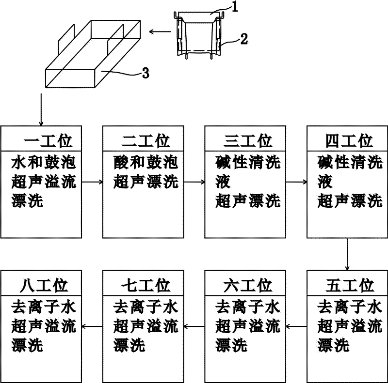
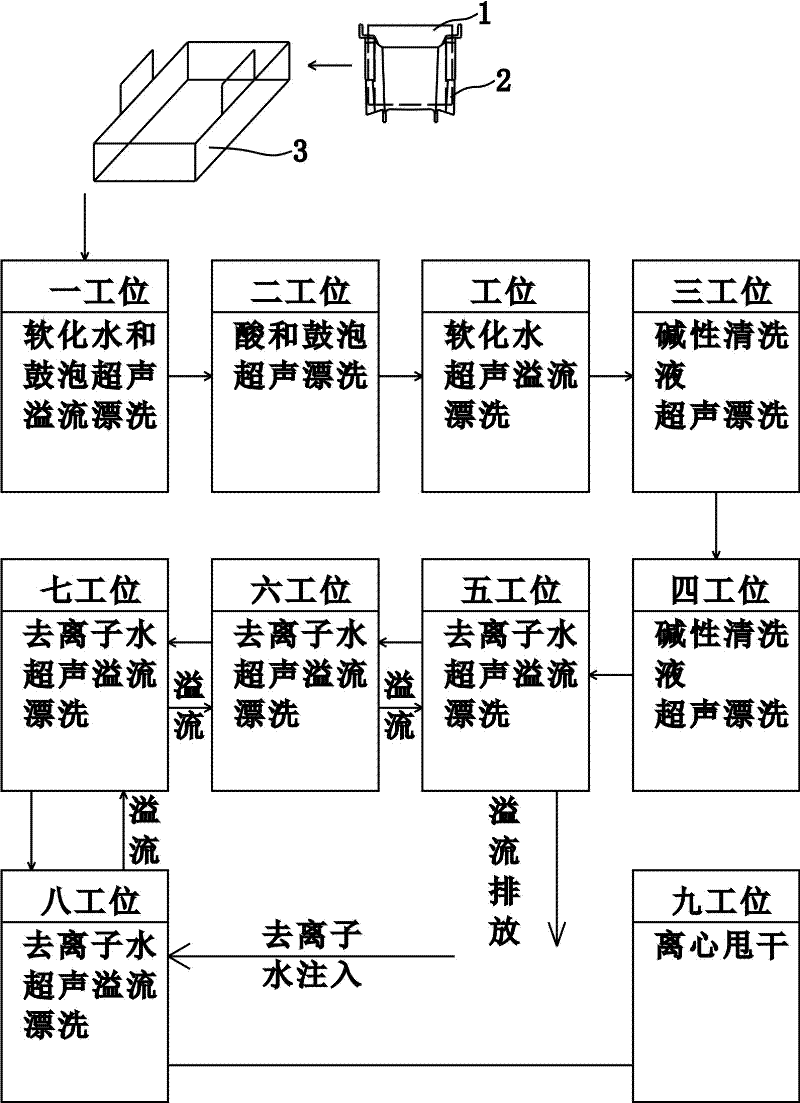
[0018] see figure 2 , this implementation case includes the silicon wafer 1, the carrier of the silicon wafer 1, that is, the flower basket 2 and the basket 3 carrying the flower basket, and the stations for cleaning the silicon wafers and completing the corresponding processes in sequence. The stations include water and bubbling ultrasonic overflow. A cleaning tank with one station for flow rinsing, a cleaning tank with two stations for ultrasonic cleaning in acid solution and bubbling, a station for ultrasonic overflow rinsing with demineralized water, a station for ultrasonic overflow cleaning with alkaline cleaning agent Three-station cleaning tank, four-station cleaning tank with alkaline cleaning agent ultrasonic cleaning tank, five-to-eight-station cleaning tank with high-frequency ultrasonic source deionized water ultrasonic overflow cleaning, equipped with nitrogen , Nine stations for centrifugal drying of silicon wafers, the temperature in the nine stations is 100~1...


PUM


Abstract

The invention discloses a cut / ground silicon wafer surface cleaning apparatus, which comprises a silicon wafer, a silicon wafer carrier and stations sequentially cleaning the silicon wafer and carrying out corresponding cleaning steps, the stations include a cleaning tank of a first station with water and bubble ultrasonic overflow rinsing, a cleaning tank of a second station with acid solution and bubble ultrasonic cleaning and the like. The cut / ground silicon wafer surface cleaning apparatus overcomes the problem of easy acid-alkali neutralization reaction, so that the PH value and concentration of the alkaline cleaner of a third station and a fourth station can be kept constant, and thereby the dirt-removing capability of the alkaline cleaner can be persistently effective. The cut / ground silicon wafers cleaned by the method have high surface cleanliness, good repeatability and a consistent color; the oxidation phenomena of mottling, bluing and blacking are prevented, and the acceptance rate of the cleaned silicon wafers is high; meanwhile, the cleaner does not need to be added in the effective period of cleaning capacity specified by the process, and the cut / ground silicon wafer surface cleaning method is easy to operate.

Description

technical field [0001] The invention relates to cutting and grinding silicon chip surface cleaning equipment. Background technique [0002] Semiconductor devices such as diodes, solar cells, and heavily doped silicon substrates for high reverse voltage transistors are directly doped and diffused on the surface of silicon cutting sheets or silicon grinding sheets to form P-N junctions and heavily doped silicon substrate layers. The surface quality of silicon wafers cannot meet the requirements for use. No matter how perfectly other process links are controlled, it is impossible to obtain high-quality semiconductor devices. The cleaning of the silicon wafer surface has become a crucial link in semiconductor silicon wafer processing and device production. In modern large-scale production, due to its large processing batch and high output, the traditional cleaning method of using cotton balls soaked in organic solvents for manual test cleaning and heating and boiling with SC-1 ...

Claims


Application Information

Patent Timeline
Patent Type & Authority Applications(China)
IPC IPC(8): H01L21/67B08B3/12B08B3/08
Inventor 汪贵发蒋建松
Owner 沈利军
Why Eureka
Try Eureka