
SiGe heterojunction triode device structure and manufacture method thereof

A triode and heterojunction technology, which is applied in semiconductor/solid-state device manufacturing, semiconductor devices, electrical components, etc., can solve the problems of affecting cut-off frequency, large gain, and small current gain, so as to improve uniformity and increase process stability , The effect of reducing process requirements

Active Publication Date: 2012-04-11
SHANGHAI HUAHONG GRACE SEMICON MFG CORP
View PDF5 Cites 4 Cited by
  • Summary
  • Abstract
  • Description
  • Claims
  • Application Information

AI Technical Summary

Problems solved by technology

If the N-type impurity in the silicon emitter diffuses too little, the current gain will be too small; otherwise, the gain will be too large, and BVceo (the breakdown voltage between the collector and the emitter when the base is open) is too small , the process stability is uncontrollable, and the diffusion of boron in the base region causes the base region to widen, which directly affects the cut-off frequency

Method used


Image

  • SiGe heterojunction triode device structure and manufacture method thereof
  • SiGe heterojunction triode device structure and manufacture method thereof
  • SiGe heterojunction triode device structure and manufacture method thereof

Examples


Embodiment Construction

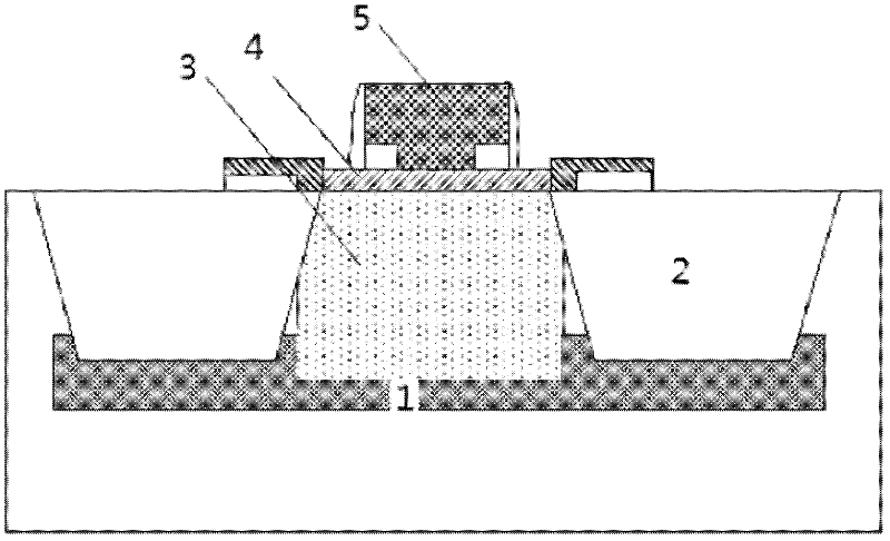
[0030] Such as figure 1 , figure 2 As shown, the silicon germanium heterojunction triode device structure of the present invention includes:

[0031] P-type substrate 1, isolation region 2, collector region 3, base region 4 and emitter region 5, collector region 2 and isolation region 3 are arranged above the P-type substrate 1, collector region 3, base region 4 and emitter region The region 5 is arranged from bottom to top from the P-type substrate 1, the base region 4 has a buffer region 6, a silicon germanium region 7 and a covering region 8 arranged in sequence, the buffer region 6 is adjacent to the collector region 3, and the covering region 8 Adjacent to the emitter region 5; wherein, the buffer region 6 and the coverage region 8 have N-type impurities.

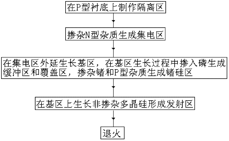
[0032] Such as image 3 As shown, an embodiment of the manufacturing method of the germanium-silicon heterojunction triode device structure of the present invention includes:

[0033] (1) making an isolation regio...


PUM


Abstract

The invention discloses a SiGe heterojunction triode device structure which comprises a P type substrate, an isolation region, a collecting zone, a base region and an emitter region. The collecting zone and the isolation region are parallel above the P type substrate. The collecting zone, the base region and the emitter region are arranged on the P type substrate from bottom to top. The base region has a buffer area, a SiGe zone and an overlay region which are arranged in order. The buffer area and the collecting zone are adjacent. The overlay region and the emitter region are adjacent. Both the overlay region and the buffer area have an N type impurity. The invention also discloses a manufacture method of the SiGe heterojunction triode device structure. According to the structure and the method in the invention, high characteristic frequency (such as more than 100 GHz) is realized, positions of a CB junction and an EB junction can be controlled accurately, adjustment of reverse withstand voltage of the EB junction is realized, base region width of a SiGe heterojunction triode can be controlled accurately, influence of base region P type ion diffusion on the base region is eliminated, and technology stability is raised.

Description

technical field [0001] The invention relates to the field of integrated circuit manufacturing, in particular to a germanium-silicon heterojunction triode device structure. The invention also relates to a manufacturing method of the germanium-silicon heterojunction triode device structure. Background technique [0002] In RF applications, higher and higher device characteristic frequencies are required. Although RFCMOS (RF Complementary Metal Oxide Semiconductor Field-Effect Transistor) can achieve higher frequencies in advanced process technologies, it is still difficult to fully meet the RF requirements, such as very It is difficult to achieve a characteristic frequency above 40GHz, and the research and development cost of advanced technology is also very high; compound semiconductors can realize very high characteristic frequency devices, but due to the disadvantages of high material cost and small size, and most compound semiconductors are toxic, it limits its applicatio...

Claims


Application Information

Patent Timeline
Patent Type & Authority Applications(China)
IPC IPC(8): H01L29/737H01L29/06H01L29/36H01L21/331
Inventor 刘冬华石晶段文婷钱文生胡君
Owner SHANGHAI HUAHONG GRACE SEMICON MFG CORP
Learn More