Processing procedure for reducing well-edge proximity effect by using curing action of photoresist

A technology of well proximity effect and curing effect, which is applied in the field of microelectronics, can solve the problem of layout area reduction and achieve the effect of increasing physical barrier and reducing WPE effect

Inactive Publication Date: 2012-04-18
SHANGHAI HUALI MICROELECTRONICS CORP
View PDF3 Cites 7 Cited by
  • Summary
  • Abstract
  • Description
  • Claims
  • Application Information

AI Technical Summary

Problems solved by technology

[0004] So far, research on how to effectively prevent the WPE effect of devices is limited to keeping the device away from the edge of the well in terms of layout, which is not conducive to the further reduction of the layout area.

Method used


Image

  • Processing procedure for reducing well-edge proximity effect by using curing action of photoresist
  • Processing procedure for reducing well-edge proximity effect by using curing action of photoresist
  • Processing procedure for reducing well-edge proximity effect by using curing action of photoresist

Examples


Embodiment Construction

[0016] The specific embodiment of the present invention will be further described below in conjunction with accompanying drawing:

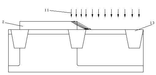
[0017] Such as Figure 2a As shown in -f, the present invention provides a process for reducing the well proximity effect by curing the photoresist, comprising the following steps:

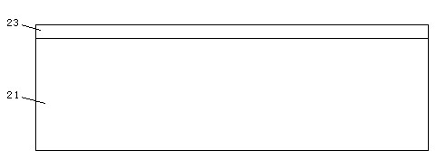
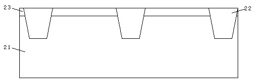
[0018] On the silicon substrate 21, an oxide layer 23 is formed by using a conventional thermal oxidation process as a barrier layer during ion implantation, wherein the thickness of the oxide layer 23 is 80-100 Å; several well regions 22 are embedded in the oxide layer 23 and the silicon substrate 21, and then dazzle the photoresist on the oxide layer 23 and the well region 22, and expose and develop the photoresist to form the photoresist 24 of the mask pattern. Wherein, the well region 22 is an N-type well, a P-type well or a deep N-type buried layer.

[0019] Further, the photoresist 24 is irradiated with UV 3 to form the shell 24 by using an ultraviolet curing ...


PUM


Abstract

The invention relates to the field of micro-electronics, in particular to a processing procedure for reducing the well-edge proximity effect by using a curing action of photoresist. According to the processing procedure for reducing the well-edge proximity effect by using the curing action of the photoresist, disclosed by the invention, ultraviolet rays radiate the surface of the photoresist to effectively cure the photoresist to form a casing layer, thereby the physical barrier of the photoresist is increased, ions radiating the photoresist are enabled to form diffuse reflection, further the implanted ions are effectively defended from scattering to the silicon surface on the edge of a photoresistor to reduce the WPE (Well-Edge Proximity Effect) of the device.

Description

technical field [0001] The invention relates to the field of microelectronics, in particular to a process for reducing well proximity effects by using photoresist curing. Background technique [0002] Well Edge-Proximity Effect (WPE for short), the root cause of which is: the implanted ions are scattered on the photoresist material, and at the edge of the photoresist, the scattered ions enter the well silicon surface, affecting the edge The doping concentration of the region; specifically, there should be three situations: 1, forming an N-type well; 2, forming a P-type well; 3, forming a deep N-type buried layer. The deep well provides a low-resistance path for latch-up protection and suppresses bipolar gain, and the deep buried layer is also the key to NMOSFET isolation triple well. However, deep buried layers affect photoresist edge devices. Some of the ions scattered on the photoresist onto the silicon surface at the edge of the photoresist, changing the threshold volta...

Claims


Application Information

Patent Timeline
Patent Type & Authority Applications(China)
IPC IPC(8): H01L21/312H01L21/336
Inventor 黄奕仙杨斌郭明升
Owner SHANGHAI HUALI MICROELECTRONICS CORP
Why Eureka
Try Eureka