Method for controlling thickness of oxidation film through ion injection process

A technology of ion implantation and oxide film, which is applied in the field of microelectronics, can solve the problems of STI edge depression and affecting device performance, etc.

Inactive Publication Date: 2012-04-18
SHANGHAI HUALI MICROELECTRONICS CORP
View PDF1 Cites 15 Cited by
  • Summary
  • Abstract
  • Description
  • Claims
  • Application Information

AI Technical Summary

Problems solved by technology

[0003] The invention discloses a special application of using ion implantation technology to control the thickness of the oxide film, which is used to solve the problem of first growing a thick oxide in the prior art, and then wet removing the area of ​​the second thick gate oxide, and then growing the second The STI edge depression caused by the gate oxide process method affects the performance of the device

Method used


Image

  • Method for controlling thickness of oxidation film through ion injection process
  • Method for controlling thickness of oxidation film through ion injection process
  • Method for controlling thickness of oxidation film through ion injection process

Examples


Embodiment Construction

[0016] The specific embodiment of the present invention will be further described below in conjunction with accompanying drawing:

[0017] A special application using ion implantation process to control the thickness of oxide film, in which,

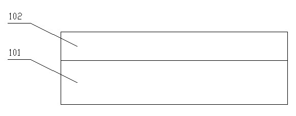
[0018] figure 1 It is a schematic diagram after spin-coating photoresist on the silicon wafer of the method for controlling the thickness of the oxide film through the ion implantation process of the present invention; please refer to figure 1 , spin-coat photoresist 102 on silicon wafer 101;

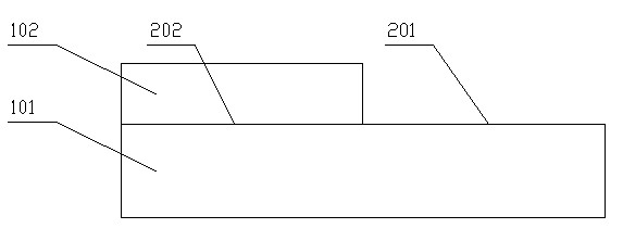
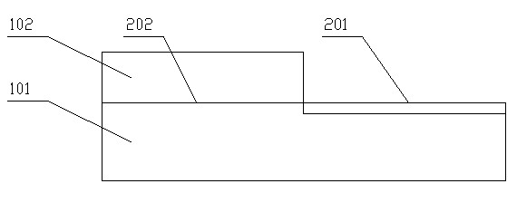
[0019] figure 2 It is a schematic diagram of the method of controlling the thickness of the oxide film through the ion implantation process of the present invention after photolithography opens the thick oxide film region, please refer to figure 2 , the thick oxide film region 201 is opened by photolithography, and the thin oxide film region 202 is covered by the remaining photoresist 102, and the thick oxide film region 201 is exposed so tha...


PUM


Abstract

The invention discloses a method for controlling the thickness of an oxidation film through an ion injection process. According to the method disclosed by the invention, the problem that the performance of a device is influenced by an STI (Shallow Trench Isolation) edge divot due to a process method of growing thick oxide, removing a region of a second kind of thickness gate oxide by adopting a wet method and growing a second kind of gate oxide is solved. The invention provides a special process method for controlling the thickness of a thermal oxidation film; the decrystallized thickness of a thick gate oxide zone on the surface of a silicon chip is controlled by injecting different energy doses; and furnace tube oxidation is subsequently carried out to grow oxidation films with various thicknesses. Since no wet-method process is used in the implementation process of the process, the STI edge divot is avoided; in addition, the oxidation films with various thicknesses can be simultaneously integrated.

Description

technical field [0001] The invention relates to a microelectronic technology, in particular to a method for controlling the thickness of an oxide film through an ion implantation process. Background technique [0002] At present, the development of semiconductors is in a diversified direction, and system-on-chip (SoC) is one of the mainstream. This means that there are multiple operating voltages on the same chip, and this type of design requires the integration of multiple thicknesses of gate oxide during chip production. The conventional integration process is to first grow a thick oxide, then wet remove the region of the gate oxide of the second thickness, and then grow the second gate oxide, and so on. Although this process is simple, it will deteriorate the STI edge divot and affect the device characteristics. Contents of the invention [0003] The invention discloses a special application of using ion implantation technology to control the thickness of the ...

Claims


Application Information

Patent Timeline
Patent Type & Authority Applications(China)
IPC IPC(8): H01L21/314H01L21/265
Inventor 景旭斌杨斌郭明升
Owner SHANGHAI HUALI MICROELECTRONICS CORP
Why Eureka
Try Eureka