
Display device and data driving circuit thereof

A data-driven circuit and display device technology, applied to static indicators, instruments, etc., can solve problems such as hard-to-implement P-type TFTs, hard-to-digital circuit amplifiers, device performance degradation, etc., to avoid resistance or capacitance arrays, and high conversion accuracy , The effect of low static power consumption

Active Publication Date: 2012-05-02
BOE TECH GRP CO LTD
View PDF3 Cites 16 Cited by
  • Summary
  • Abstract
  • Description
  • Claims
  • Application Information

AI Technical Summary

Problems solved by technology

The current oxide TFTs have the following characteristics: (1) oxide TFTs are generally N-type devices, and it is difficult to realize P-type TFTs, so it is difficult to realize CMOS-type digital circuits or amplifiers; (2) the mobility of oxide TFTs is lower than that of The mobility of single crystal silicon is 2 or more orders of magnitude smaller, so it is necessary to improve the circuit structure to increase the working speed of the integrated oxide TFT circuit; (3) The oxide TFT may degrade the device performance after working for a long time
Therefore, the data driving circuit design scheme developed based on single crystal silicon CMOS technology cannot be directly used in the data driving circuit design of oxide TFT

Method used


Image

  • Display device and data driving circuit thereof
  • Display device and data driving circuit thereof
  • Display device and data driving circuit thereof

Examples


Embodiment 1

[0034] Such as Figure 4 As shown, it is a functional block diagram of the DAC of this embodiment, including: a voltage subdivision module 41 for obtaining detailed analog voltage values ​​to realize DAC conversion with more digits and higher resolution. The voltage subdivision module includes a reset unit, a decoding preset unit, a decoding unit and a charge sharing unit; wherein, the reset unit couples the potential of the reference load capacitance and the conversion load capacitance to the first voltage; the decoding preset unit pre-decodes the reference load The capacitor is set to the first voltage or the second voltage; the decoding unit performs time-division and bit-by-bit conversion according to the input digital signal to obtain the potential state on the reference load capacitor; the charge sharing unit uses the principle of charge redistribution to convert the reference load The capacitance and the conversion load capacitance are converted to obtain the analog vol...

Embodiment 2

[0040] Figure 6 A functional block diagram of the DAC of this embodiment is schematically described, including: a voltage selection module 61 and a voltage subdivision module 62 . The voltage selection module 61 selects a corresponding reference voltage source under the action of the first group of digital selection signals Bns. Since the voltage subdivision module 62 needs to use a lower first selection voltage V L and the higher second selection voltage V H , so the voltage selection module 41 includes generating the first selection voltage V L The first voltage selection module and generates the second selection voltage V H The second voltage selection module. The voltage subdivision module 62 generates the output voltage V under the action of the second group of digital selection signals Bms O . The output voltage V O The magnitude of the first selection voltage is between V L and the second selection voltage V H between. The 6-bit DAC is still taken as an examp...


PUM


Abstract

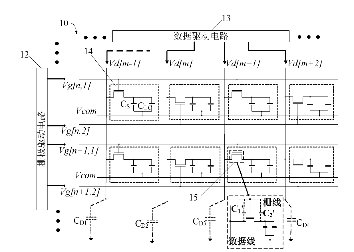
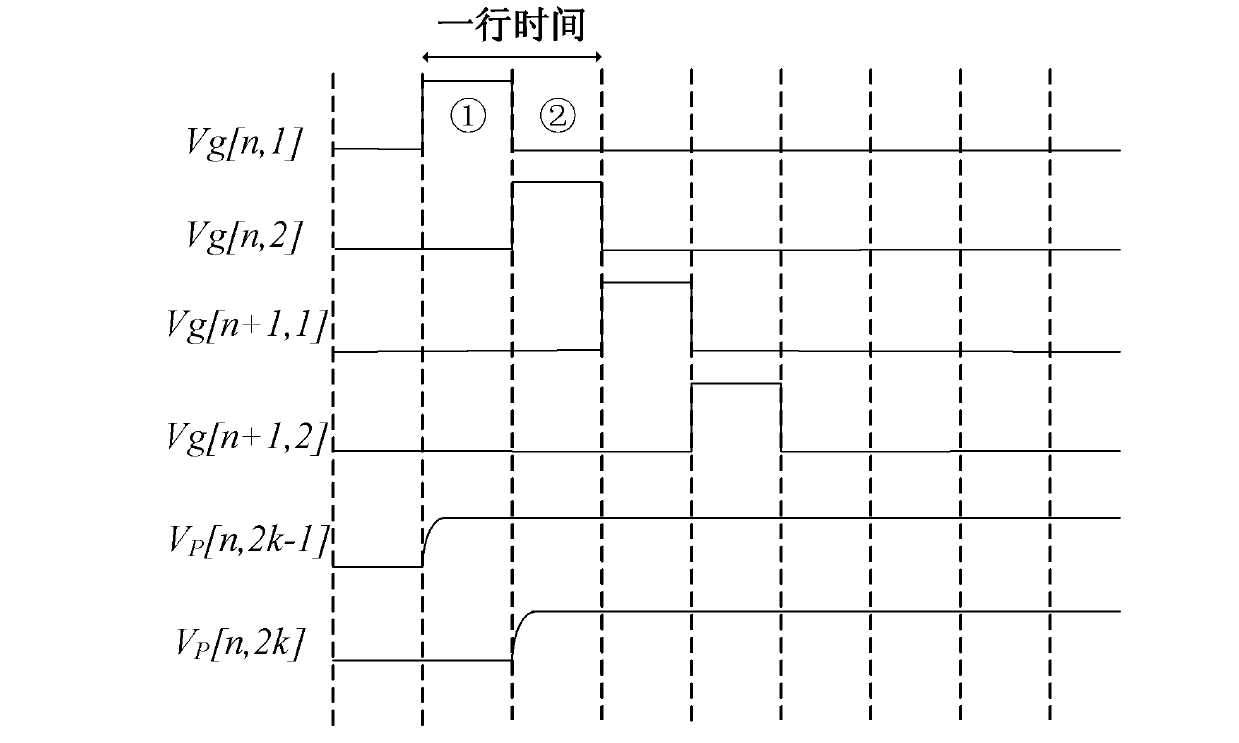
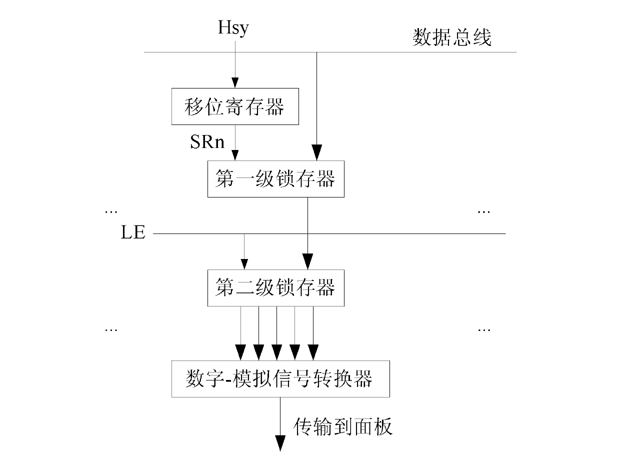
The invention discloses a display device and a data driving circuit adopted by the display device. The display device comprises a panel, a gate driving circuit and the data driving circuit, wherein the panel comprises a two-dimensional pixel matrix composed of multiple pixels, and multiple first-direction data lines and multiple second-direction gate scanning lines; the multiple first-direction data lines and the multiple second-direction gate scanning lines are connected with each pixel; the data driving circuit is used for providing an image signal from the data lines; the gate driving circuit is used for providing a scanning signal for the gate scanning lines; and the data lines can be divided into N groups, and the data lines in the same group share the same gate scanning line. In the invention, all transistors in a DAC (digital-to-analog converter) only realize a switching action, the accuracy of the DAC is determined by the ratio of a load capacitor on adjacent data lines, and the ratio of the load capacitor on the adjacent data lines on a display panel are more accurate, thus the output voltage of the data driving circuit is more accurate.

Description

technical field [0001] The present invention relates to a display device, in particular to a display device and a data driving circuit adopted therefor. Background technique [0002] TFT (Thin Film Transistor, thin film transistor) technology is the mainstream of today's flat panel display technology. The main markets of flat panel display technology include: mobile displays such as mobile phones, mobile DVDs, PSP (Play Station Portable), notebooks, etc., or monitor displays, TV displays, etc. In the design of these display devices, how to optimize the display effect and reduce the cost and power consumption of the display device is the most important goal. Fully integrated TFT panel design is an important technology to control cost and reduce power consumption, which has received close attention in recent years. The so-called fully integrated TFT panel design mainly refers to the design of integrating gate drive circuits, data drive circuits and other peripheral circuits ...

Claims


Application Information

Patent Timeline
Patent Type & Authority Applications(China)
IPC IPC(8): G09G3/36
Inventor 张盛东廖聪维陈韬刘晓明
Owner BOE TECH GRP CO LTD
Learn More