Method and device for monitoring pretreatment in low-dielectric-constant barrier layer process

A low dielectric constant, pretreatment technology, applied in circuits, electrical components, complex mathematical operations, etc., can solve the problems affecting the adhesion of the dielectric layer and the copper connection, affecting the reliability and stability of the product, and improve reliability. Effects on stability, failure prevention, and adhesion prevention

Active Publication Date: 2012-05-02
SHANGHAI HUALI MICROELECTRONICS CORP
View PDF3 Cites 8 Cited by
  • Summary
  • Abstract
  • Description
  • Claims
  • Application Information

AI Technical Summary

Problems solved by technology

Therefore, if the pretreatment in the low dielectric constant barrier layer process fails, it will directly affect the adhesion between the dielectric layer and the copper wiring, thereby affecting the reliability and stability of the product

Method used


Image

  • Method and device for monitoring pretreatment in low-dielectric-constant barrier layer process
  • Method and device for monitoring pretreatment in low-dielectric-constant barrier layer process
  • Method and device for monitoring pretreatment in low-dielectric-constant barrier layer process

Examples


Embodiment Construction

[0015] Specific embodiments of the present invention will be described in detail below in conjunction with the accompanying drawings. It should be noted that the embodiments described here are for illustration only, and are not intended to limit the present invention.

[0016] For traditional monitoring methods, see Table 1 below:

[0017]

[0018] Table 1

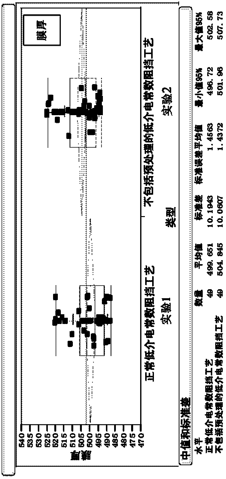
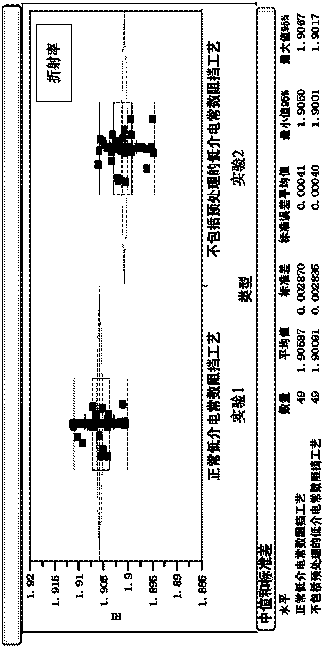
[0019] The monitoring method of the present invention has increased the monitoring of an independent pretreatment than traditional monitoring method, see following table 2:

[0020]

[0021] Table 2

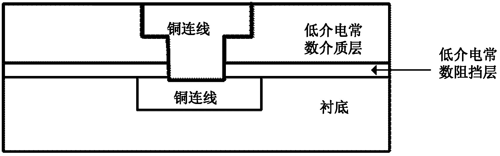
[0022] Comparing the present invention with the traditional monitoring method, the present invention provides a pretreatment monitoring method in the low dielectric constant barrier layer process. In detail, the present invention manufactures products (such as figure 1 In-process timing (e.g., 24 hours as a cycle) of the product shown) performs a separate pretreatment process on the wafer (silicon substrate) in the ...


PUM


Abstract

The invention provides a method and a device monitoring pretreatment in a low-dielectric-constant barrier layer process. The method comprises the following steps of: detecting a plurality of film parameters of a silicon substrate which is subjected to pretreatment at different times; establishing a statistic process control curve according to the plurality of film parameters; setting a control line with a preset threshold value; if the range of the statistic process control curve is within the threshold value, judging that the pretreatment is normal; and if the range of the statistic process control curve exceeds the threshold value, judging that the pretreatment is abnormal. The method and the device can be used for effectively preventing invalidation of a pretreatment process so as to improve the reliability and the stability of a product.

Description

technical field [0001] The present invention relates to the field of semiconductor manufacturing, in particular to a method and device for monitoring pretreatment (treatment) in a low dielectric constant barrier layer (low-K block) process. Background technique [0002] When the semiconductor process enters the stage of copper interconnection technology, a low dielectric constant barrier layer needs to be used between the copper wiring and the low dielectric constant dielectric layer as a barrier layer for the damascene etching process on the dielectric layer. In the semiconductor manufacturing industry, the mainstream low dielectric constant barrier layer process is Nitrogen-doped carbon (NDC, Nitrogen-doped carbon) and N-barrier layer process. Because copper is exposed to the air, it is easy to form copper oxide (CuO 2 ), so in the low dielectric constant barrier layer process, a pretreatment step is required before the deposition of the low dielectric constant barrier la...

Claims


Application Information

Patent Timeline
Patent Type & Authority Applications(China)
IPC IPC(8): H01L21/66H01L21/67
CPCH01L22/12G06F17/18G07C3/14H01L22/20
Inventor 顾梅梅李建张景春
Owner SHANGHAI HUALI MICROELECTRONICS CORP
Why Eureka
Try Eureka