Supercharge Your Innovation With Domain-Expert AI Agents!

Novel Schottky flip-chip and manufacturing process thereof

A manufacturing process and flip-package technology, applied in the field of new Schottky flip-package chips and manufacturing processes, can solve the problems of short distance, low isolation, increased thickness, etc., to improve product work efficiency and meet high precision requirements, the effect of improving isolation performance

Active Publication Date: 2013-09-04
CHONGQING PINGWEI ENTERPRISE
View PDF4 Cites 0 Cited by
  • Summary
  • Abstract
  • Description
  • Claims
  • Application Information

AI Technical Summary

Problems solved by technology

On the one hand, this structure increases the thickness of the product because of the raised connection end, and its adaptability is getting worse and worse in the modern society when the volume of electronic products is getting smaller and smaller; on the other hand, the positive electrode and the The distance between the negative poles is not far and has not been isolated, so the isolation effect between the positive and negative poles of the output terminal is not very good. When used in some high-demand circuits, it will be damaged due to the isolation between the positive and negative poles Not high enough to meet usage requirements

Method used


Image

  • Novel Schottky flip-chip and manufacturing process thereof
  • Novel Schottky flip-chip and manufacturing process thereof
  • Novel Schottky flip-chip and manufacturing process thereof

Examples


Embodiment Construction

[0025] Below in conjunction with accompanying drawing, the present invention is described in further detail:

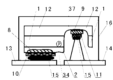
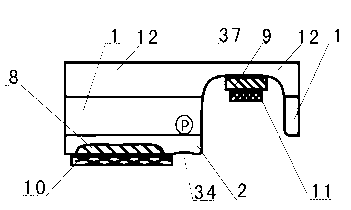
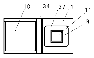
[0026] Such as figure 1 , figure 2 with image 3 As shown, the novel Schottky flip-pack chip in the present invention includes package body 16, chip positive pole 13, chip negative pole 14, silicon wafer 12, silicon wafer positive pole 10 and silicon wafer negative pole 11, and the total thickness of package body 16 is 0.6- 0.7mm; the silicon wafer positive pole 10 is connected to the chip positive pole 13, and the silicon wafer negative pole 11 is connected to the chip negative pole 14; the silicon wafer positive pole 10 and the silicon wafer negative pole 11 are located on the same side of the silicon wafer 12 ( figure 1 with figure 2 The positive electrode 10 of the silicon wafer is located on the surface of the silicon wafer 12, and a groove 37 is arranged beside the positive electrode 10 of the silicon wafer, and the negative electrode 11 of the silicon wafe...


PUM


Abstract

The invention discloses a novel Schottky flip-chip which comprises a packaging body, a chip anode, a chip cathode, a silicon chip, a silicon chip anode and a silicon chip cathode. The silicon chip anode is connected with the chip anode. The silicon chip cathode is connected with the chip cathode. The silicon chip anode and the silicon chip cathode are positioned at a same side surface of the silicon chip. The silicon chip anode is on a surface of the silicon chip. A groove is provided beside the silicon chip anode. The silicon chip cathode is positioned in the groove. The invention also discloses manufacturing process of the novel Schottky flip-chip. The manufacturing process comprises the following steps: providing an original epitaxial silicon chip; carrying out oxidation on the original epitaxial silicon chip; carrying out photoetching for the first time; carrying out p-ring diffusion; carrying out photoetching groove for the second time; carrying out photoetching for the third time; carrying out corrosion for the first time, sputtering metal Pt and Ni; evaporating contact metal Ti, Ni and Ag; carrying out soldering tin and packaging to obtain a finished product. The novel Schottky flip-chip has the advantages of a small volume, thinness and good performance.

Description

technical field [0001] The invention relates to a Schottky flip-package chip and a manufacturing process, in particular to a novel Schottky flip-package chip with positive and negative electrodes located on the same side and a negative electrode concave inward, and a manufacturing process. Background technique [0002] Schottky flip-pack chip is a Schottky chip produced by flip-package technology. At present, the flip-package of the chip adopts solder ball technology. When it comes to the important role of electrical interconnection and mechanical support, it is an ideal packaging technology. [0003] Currently, the Schottky chip processed by solder ball technology has a structure in which raised solder balls are arranged on the surface of the silicon wafer as the positive and negative electrodes of the chip. On the one hand, this structure increases the thickness of the product because of the raised connection end, and its adaptability is getting worse and worse in the mod...

Claims


Application Information

Patent Timeline
Patent Type & Authority Patents(China)
IPC IPC(8): H01L29/41H01L29/872H01L21/329
Inventor 王兴龙李述州
Owner CHONGQING PINGWEI ENTERPRISE
Features
  • R&D
  • Intellectual Property
  • Life Sciences
  • Materials
  • Tech Scout
  • Unparalleled Data Quality
  • Higher Quality Content
  • 60% Fewer Hallucinations
Learn More