Optical structure to reduce internal reflections and method thereof
一种内部反射、光学系统的技术,应用在光学系统领域,能够解决图像降级等问题
- Summary
- Abstract
- Description
- Claims
- Application Information
AI Technical Summary
Problems solved by technology
Method used
Image

Examples
Embodiment 1
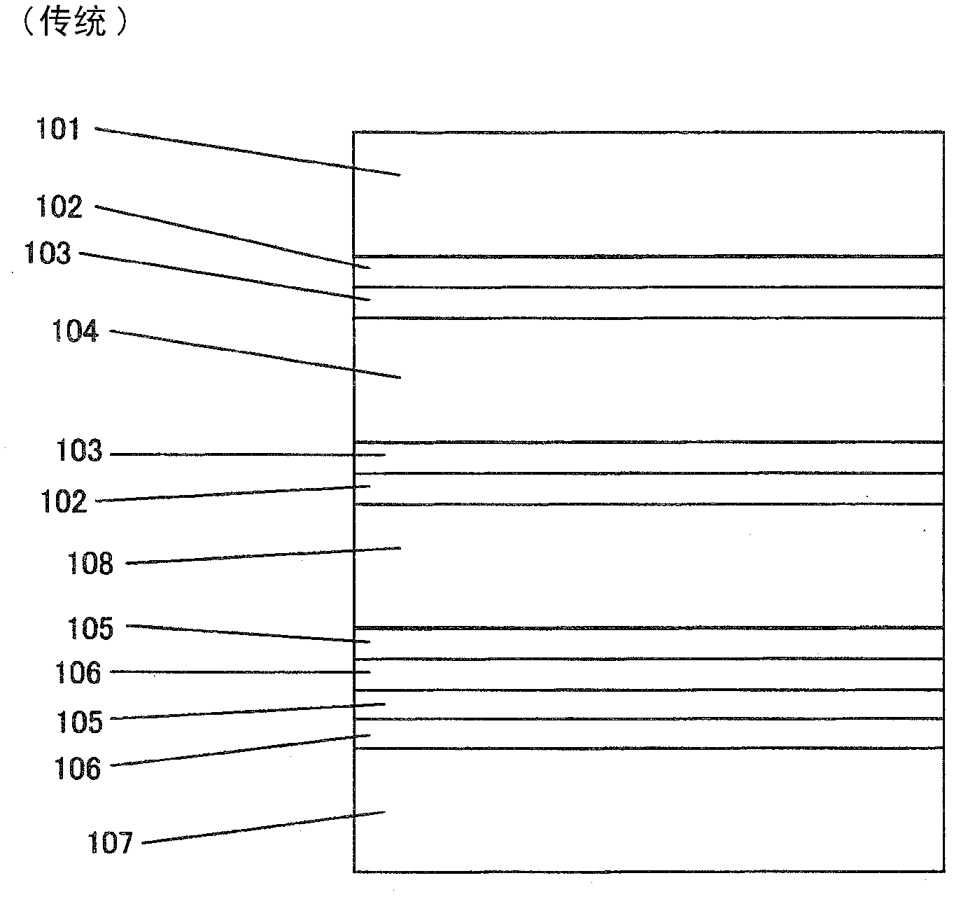
[0062] refer to figure 1 , describes an example of an optical structure that can be implemented as a liquid crystal display (LCD), where one ITO electrode 102 of n ≈ 1.95 is located between a liquid crystal layer (LC) 104 of n ≈ 1.53 and a glass or color filter (CF) 101 of n ≈ 1.53 and another ITO electrode is located between the LC 104 and the flat resin 108 with n≈1.59. Between the LC and each ITO electrode there is also a thin layer 103 of polyimide (PI) with n≈1.70. Between the silicon dioxide layer 106 of n≈1.55 and / or between the silicon dioxide layer 106 and the planar resin layer, there is also a silicon nitride layer 105 of n≈2.04. The silicon dioxide and silicon nitride layers serve as dielectric and passivation functions in and around the TFT system. Glass 107 supports the structure (another type of support could be eg a polymer (eg a polymer substrate)). This is a typical structure used in the industry and is described in Table 1, along with the thickness of eac...
Embodiment 2
[0077] Silicon dioxide and / or silicon nitride may also be removed from the areas of the LCD through which light is transmitted. This is because they are only necessary around TFTs and circuitry within the device. Light is not transmitted through these areas (light is either reflected by the metal or absorbed in commonly used black shades), so they can be considered irrelevant for the purpose of reducing internal reflections. Silicon dioxide and silicon nitride can in principle be patterned such that they are only found in these opaque areas and not in the transparent parts of the pixels. In this case, the structure is shown in Table 4 and Figure 7 shown.
[0078] The structure described in Table 3 optimizes the thickness of PI and ITO to minimize the total reflectance through destructive interference. The total reflectance of this structure is 0.015; 1.5% of the incident light is reflected by this internal structure.
[0079] Table 4
[0080] Material
Fig...
PUM
| Property | Measurement | Unit |
|---|---|---|
| reflectivity | aaaaa | aaaaa |
| refractive index | aaaaa | aaaaa |
| refractive index | aaaaa | aaaaa |
Abstract
Description
Claims
Application Information
 - R&D
- Intellectual Property
- Life Sciences
- Materials
- Tech Scout
- Unparalleled Data Quality
- Higher Quality Content
- 60% Fewer Hallucinations
Browse by: Latest US Patents, China's latest patents, Technical Efficacy Thesaurus, Application Domain, Technology Topic, Popular Technical Reports.
© 2025 PatSnap. All rights reserved.Legal|Privacy policy|Modern Slavery Act Transparency Statement|Sitemap|About US| Contact US: help@patsnap.com