Method for forming interconnecting groove and through hole and method for forming interconnecting structure

An interconnection structure and trench technology, which is applied in electrical components, semiconductor/solid-state device manufacturing, circuits, etc., can solve the problems of hydrofluoric acid corrosion of cobalt-tungsten-phosphorus copper, increase of k value, and damage of ultra-low-k dielectric layer, etc.

Active Publication Date: 2012-05-09
SEMICON MFG INT (SHANGHAI) CORP +1
View PDF6 Cites 15 Cited by
  • Summary
  • Abstract
  • Description
  • Claims
  • Application Information

AI Technical Summary

Problems solved by technology

However, when cleaning the interconnect trench 21 and the via hole 22, hydrofluoric acid will corrode cobalt-tungsten-phosphorus and copper
Moreover, in the method for forming interconnection trenches and through holes described above, when etching to form interconnection trenches and through holes, the method used is dry etching, and the plasma bombards the dielectric layer in the dry etching process. , it will damage the ultra-low-k dielectric layer, resulting in an increase in the k value
[0006] In the prior art, there are many methods for forming interconnection trenches and via holes, such as the method disclosed in Chinese patent application with publication number CN101055421A, but none of them solves the above-mentioned problems

Method used


Image

  • Method for forming interconnecting groove and through hole and method for forming interconnecting structure
  • Method for forming interconnecting groove and through hole and method for forming interconnecting structure
  • Method for forming interconnecting groove and through hole and method for forming interconnecting structure

Examples


Embodiment Construction

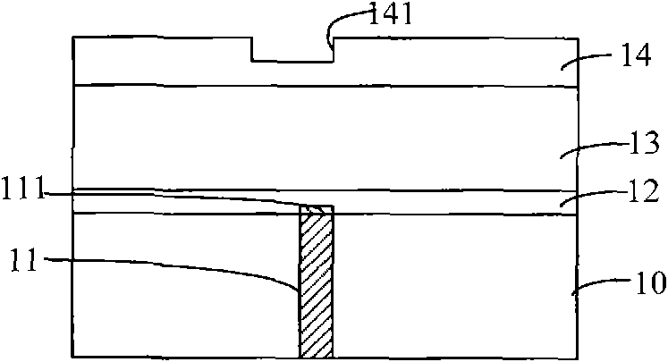
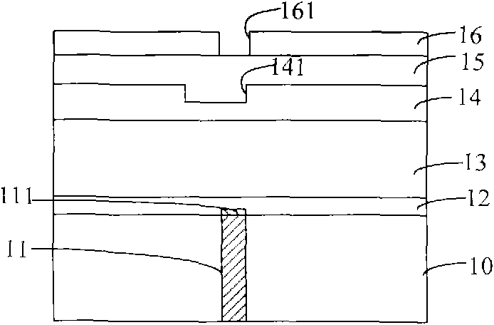
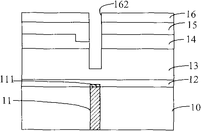
[0046] In the method for forming interconnect trenches and via holes according to specific embodiments of the present invention, in the process of forming interconnect trenches and via holes in the dielectric layer, the etch stop layer is not removed, and the etch stop layer separates the cap layer from the acid isolation so the acid does not corrode the cap layer as well as the copper. Afterwards, the etch stop layer is removed, and then the interconnection trenches and through holes are processed. The treatment method is: irradiating the interconnection trenches and through holes with ultraviolet rays, and injecting into the interconnection trenches and through holes. Ozone gas and water vapor, and then use an organic solvent to clean the interconnection trenches and via holes.

[0047] In order to enable those skilled in the art to better understand the present invention, specific embodiments of the present invention will be described in detail below in conjunction with the...


PUM

PropertyMeasurementUnit
Thicknessaaaaaaaaaa

Abstract

The invention relates to a method for forming an interconnecting groove and a through hole and a method for forming an interconnecting structure. The method for forming the interconnecting groove and the through hole comprises the following steps that: a substrate is provided, a dielectric layer having a copper plug is formed on the substrate, and a cap layer is formed on the copper plug; an etching stopping layer is respectively formed on the surface of the dielectric layer of the copper plug and the surface of the cap layer, and a dielectric layer is formed on the etching stopping layer; the interconnecting groove and the through hole are formed on the dielectric layer; the interconnecting groove and the through hole are cleaned by acid; and the etching stopping layer covering the surface of the cap layer is removed in a dry etching way. The interconnecting groove and the through hole are radiated by ultraviolet; the interconnecting groove and the through hole stay in an ozone gas and water vapor atmosphere; and the interconnecting groove and the through hole are cleaned by organic solvent. Due to the adoption of the method, the cap layer is free from being corroded, and the damaged dielectric layer can be repaired.

Description

technical field [0001] The invention relates to the technical field of semiconductors, in particular to methods for forming interconnection trenches, through holes and interconnection structures. Background technique [0002] With the development of semiconductor technology, semiconductor devices are becoming smaller and smaller. In the process below 32 nanometers (nm), there is an electronic migration (EM) problem in the back end of line (BEOL). In order to solve the problem of electromigration, the existing solution is to use copper plugs Cobalt Tungsten Phosphorus (CoWP) is formed to prevent electromigration problems. [0003] After forming cobalt-tungsten-phosphorus, when continuing to form the interconnection structure connected with the copper plug on the copper plug, it is necessary to form interconnection trenches and vias on the copper plug covered with cobalt-tungsten-phosphorus (using a dual damascene process) . [0004] refer to Figure 1a ~ Figure 1d , in the...

Claims


Application Information

Patent Timeline
IPC IPC(8): H01L21/768H01L21/26H01L21/02
Inventor 张海洋李凡
Owner SEMICON MFG INT (SHANGHAI) CORP
Why Eureka
Try Eureka