DIP (dual in-line package) component electrostatic protector

A technology of double in-line insertion and components, applied in the direction of electrical components, electric solid devices, semiconductor devices, etc., can solve problems such as component failure, and achieve convenient storage and good use effect

Inactive Publication Date: 2012-05-09
铜陵浩岩节能科技有限公司
View PDF3 Cites 1 Cited by
  • Summary
  • Abstract
  • Description
  • Claims
  • Application Information

AI Technical Summary

Problems solved by technology

For field effect components in DIP packages, the failure ...

Method used


Image

  • DIP (dual in-line package) component electrostatic protector
  • DIP (dual in-line package) component electrostatic protector
  • DIP (dual in-line package) component electrostatic protector

Examples


Embodiment Construction

[0013] The content of the present invention will be described below in conjunction with specific embodiments.

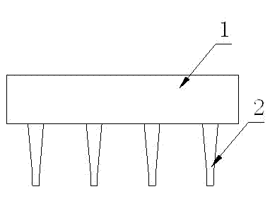
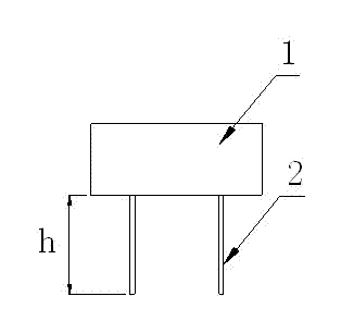
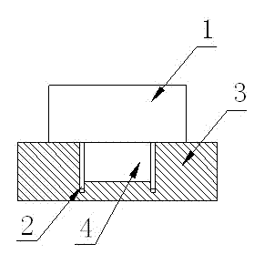
[0014] like figure 1 As shown, it is the front view of the dual-in-line component described in the present invention, figure 2 for its left view. The dual in-line component of the present invention includes a body 1 and lead pins 2 . The lead pins 2 are double rows, symmetrically distributed on one side of the body 1 . The lead pins 2 are fixed on the body 1, and the body 1 uses the lead pins 2 to contact the printed circuit board, and then access the circuit to work.

[0015] Since field effect components are prone to static electricity during packaging, transportation or operation, and field effect components have high input impedance, it is difficult to release the static electricity generated by the induced electric field and friction. It is easy to cause circuit breakdown in the main body 1, which directly affects the utilization rate of field effect compon...


PUM


Abstract

The invention relates to a DIP (dual in-line package) component electrostatic protector. The electrostatic protector comprises a shell, wherein the shell is provided with a groove, the width of a body is greater than that of the groove, the length of a terminal pin is less than the depth of the groove, the groove of the shell is internally provided with a bulge, the hole between the bulge and the side wall of the groove and the terminal pin are in interference fit with each other, and the contact part of the bulge and the terminal pin can conduct electricity. The DIP component electrostatic protector provided by the invention has the advantages that a DIP terminal pin structure is utilized, so that static breakdown caused by welding friction, induction and the like before the component is connected with an electronic circuit and then powered on can be fundamentally and completely eradicated, and the storage, transportation, operation, use and the like of the component can be carried out conveniently. The electrostatic protector has no special requirement on welding tools and workshop environment, can be used repeatedly and has a good practical effect.

Description

technical field [0001] The invention relates to an electrostatic protector, in particular to an electrostatic protector for double in-line field effect components. Background technique [0002] Field effect components are the abbreviation of metal oxide semiconductor field effect integrated circuits, which can be divided into CMOS (Complementary Metal Oxide Semiconductor, complementary metal oxide semiconductor), PMOS (P-Channel Metal Oxide Semiconductor, P channel metal oxide semiconductor) , NMOS (N-Channel Metal Oxide Semiconductor, N-channel Metal Oxide Semiconductor) and other structural forms. Because of its low power consumption, wide operating voltage range, strong anti-interference ability, large logic swing, high input impedance, strong output capability, and low cost, it is widely used in space electronic equipment, military and civilian electronic products, and industrial control In equipment, the amount of usage is second only to ordinary integrated circuits. ...

Claims


Application Information

Patent Timeline
IPC IPC(8): H01L23/60
Inventor 杨镇
Owner 铜陵浩岩节能科技有限公司
Why Eureka
Try Eureka