Thin film solar battery and manufacturing method thereof

A technology of solar cells and manufacturing methods, which is applied to circuits, photovoltaic power generation, electrical components, etc., can solve the problems of reducing the bandgap width of thin-film solar cells, reducing the photoelectric conversion efficiency of thin-film solar cells, and polluting single-crystal silicon substrates, etc., to achieve Improve photoelectric conversion efficiency, reduce pollution, and increase the effect of bandgap width

Inactive Publication Date: 2012-05-09
SILEVO CHINA
View PDF6 Cites 3 Cited by
  • Summary
  • Abstract
  • Description
  • Claims
  • Application Information

AI Technical Summary

Problems solved by technology

[0006] But there is following defect in above-mentioned technology: when the doping concentration of the phosphorus ion in the phosphorus-doped layer 3 or the boron ion in the boron-doped layer 5 is higher, then the phosphorus-doped layer 3 or the boron-doped layer 5 will pollute the monocrystalline silicon substrate 4, thereby reducing the photoelectric conversion efficiency of the thin-film solar cell; when the doping concentration of the phosphorus ion in the phosphorus-doped layer 3 or the boron ion in the boron-doped layer 5 is low, the bandgap width of the thin-film solar cell will be reduced, thereby It will also reduce the photoelectric conversion efficiency of thin-film solar cells

Method used


Image

  • Thin film solar battery and manufacturing method thereof
  • Thin film solar battery and manufacturing method thereof
  • Thin film solar battery and manufacturing method thereof

Examples


Embodiment 1

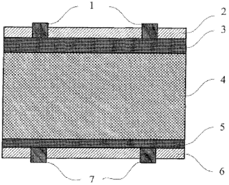
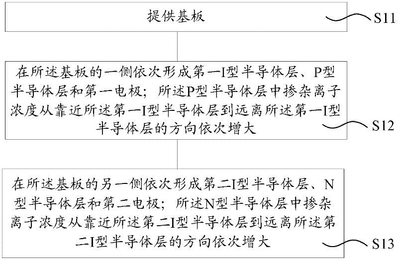
[0068] refer to figure 2 As shown, the present embodiment provides a method for manufacturing a thin-film solar cell, including:

[0069] Step S11, providing a substrate;

[0070] Step S12, sequentially forming a first I-type semiconductor layer, a P-type semiconductor layer, and a first electrode on one side of the substrate; the concentration of dopant ions in the P-type semiconductor layer ranges from close to the first I-type semiconductor layer to The direction away from the first I-type semiconductor layer increases sequentially;

[0071] Step S13, forming a second I-type semiconductor layer, an N-type semiconductor layer and a second electrode in sequence on the other side of the substrate; the concentration of dopant ions in the N-type semiconductor layer is from close to the second I-type semiconductor layer The direction away from the second I-type semiconductor layer increases sequentially.

[0072] In this embodiment, the pollution of the P-type semiconductor l...

Embodiment 2

[0124] This embodiment provides a method for manufacturing a thin-film solar cell, including:

[0125] Provide the substrate;

[0126] An I-type semiconductor layer and a P-type semiconductor layer are sequentially formed on the substrate, and the concentration of dopant ions in the P-type semiconductor layer increases sequentially from a direction close to the I-type semiconductor layer to a direction away from the I-type semiconductor layer.

[0127] Wherein, the substrate may be an N-type substrate.

[0128] The steps of forming the I-type semiconductor layer and the P-type semiconductor layer are the same as the steps of forming the first I-type semiconductor layer and the P-type semiconductor layer in Embodiment 1, and will not be repeated here.

[0129] After the P-type semiconductor layer is formed, an anti-reflection layer and a front electrode can be sequentially formed on the P-type semiconductor layer, and a back electrode can be formed on the lower surface of the ...

Embodiment 3

[0138] This embodiment provides a method for manufacturing a thin-film solar cell. The difference between it and Embodiment 2 is that in this embodiment, an N-type semiconductor layer is formed on the P-type semiconductor layer after the P-type semiconductor layer is formed.

[0139] Wherein, the concentration of dopant ions in the N-type semiconductor layer may be distributed uniformly or unevenly, which does not limit the protection scope of the present invention.

[0140] Specifically, refer to Figure 13 As shown, the thin-film solar film cell made by the method of this embodiment includes:

[0141] Substrate 30;

[0142] I-type semiconductor layer 31, P-type semiconductor layer 32, N-type semiconductor layer 33, anti-reflection layer 34 and front electrode 35 located on the upper surface of the substrate 30 in sequence;

[0143] The back electrode 36 located on the lower surface of the substrate 20 .

[0144] Wherein, the substrate 30 may be an N-type substrate or a P-...


PUM


Abstract

The invention relates to a thin film solar battery and a manufacturing method thereof. The thin film solar battery comprises a substrate, a first I-type semiconductor layer, a P-type semiconductor layer and a first electrode, a second I-type semiconductor layer, an N-type semiconductor layer and a second electrode, wherein the first I-type semiconductor layer, the P-type semiconductor layer and the first electrode are positioned at one side of the substrate in sequence, and the concentration of ions doped in the P-type semiconductor layer successively increases from the direction adjacent to the first I-type semiconductor layer to the direction far away from the first I-type semiconductor layer; the second I-type semiconductor layer, the N-type semiconductor layer and the second electrode are positioned at the other side of the substrate in sequence, and the concentration of ions doped in the N-type semiconductor layer successively increases from the direction adjacent to the second I-type semiconductor layer to the direction far away from the second I-type semiconductor layer. The invention has the beneficial effect that not only can the pollution of the P-type semiconductor layers or the N-type semiconductor layers to the I-type semiconductor layers be reduced, but also the larger band gap width can be obtained, and therefore, the photoelectric conversion efficiency is high.

Description

technical field [0001] The invention relates to the technical field of thin-film solar cells, in particular to a thin-film solar cell and a manufacturing method thereof. Background technique [0002] Thin-film solar cells are solar cells formed by depositing very thin (several micrometers to tens of micrometers) photoelectric materials on substrates such as glass, metal or plastic. Thin-film solar cells have a series of advantages such as power generation under weak light conditions, low energy consumption in the production process, and can greatly reduce raw material and manufacturing costs. They have become a research hotspot in recent years, and their market development potential is huge. [0003] Basic thin film solar cell structure, including single P-N junction, P-I-N / N-I-P and multi-junction. A typical single-junction P-N structure includes a P-type doped layer and an N-type doped layer. Single-junction P-N junction solar cells have two structures: homojunction and ...

Claims


Application Information

Patent Timeline
IPC IPC(8): H01L31/0352H01L31/077H01L31/20
CPCY02E10/50Y02E10/547Y02P70/50
Inventor 傅建明杨瑞鹏
Owner SILEVO CHINA
Why Eureka
Try Eureka