Preparation method for silicon germanium (SiGe) monitoring chip and monitoring method adopting chip

A technology of monitor sheet and grating graphics, which is applied in semiconductor/solid-state device manufacturing, electrical components, electric solid-state devices, etc., can solve problems such as high cost of measuring equipment, unsuitable for production, and inability to characterize, so as to improve process control ability and reduce Monitoring cost, effect of high sensitivity

Active Publication Date: 2012-05-16
SHANGHAI HUAHONG GRACE SEMICON MFG CORP
View PDF4 Cites 2 Cited by
  • Summary
  • Abstract
  • Description
  • Claims
  • Application Information

AI Technical Summary

Problems solved by technology

But usually this change is too weak to be directly characterized by planar thin films
Although methods such as Raman spectroscopy can detect the change of the lattice through the collision and scattering of photons and the lattice, the cost of the measurement equipment is very high, and it requires the measurement personnel to have strong optical and solid-state technology and theoretical knowledge. Model establishment and calibration, in addition, strong mathematical analysis capabilities are required to perform measurement data and interpret Raman spectra, and there are very few such professional and technical personnel, so this method is usually only suitable for some large scientific research institutes and universities. For scientific research, not suitable for production

Method used


Image

  • Preparation method for silicon germanium (SiGe) monitoring chip and monitoring method adopting chip
  • Preparation method for silicon germanium (SiGe) monitoring chip and monitoring method adopting chip
  • Preparation method for silicon germanium (SiGe) monitoring chip and monitoring method adopting chip

Examples


Embodiment Construction

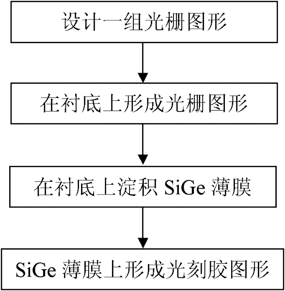
[0026] The preparation method of SiGe monitoring sheet of the present invention, this SiGe monitoring sheet is used for monitoring the content of SiGe thin film, comprises the steps (see figure 1 ):

[0027] 1) At least one set of grating graphics is designed; the lithography graphics can be regularly arranged line graphics, or regularly arranged box-like dot matrix graphics. The spatial period of the grating pattern is 0.1-100 microns, preferably 1-20 microns.

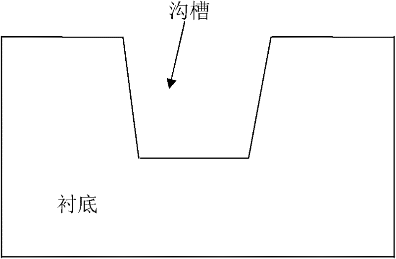
[0028] 2) Define the grating pattern in step 1 on the substrate (which can be a silicon substrate), and etch the substrate to form a grating pattern with a step difference (see image 3 ); that is, to form a grating pattern composed of a plurality of regularly arranged grooves.

[0029] 3) Depositing a SiGe film with a specific content on the substrate to form a SiGe film grating pattern;

[0030] 4) adopt photolithography process, keep photoresist in the middle of groove bottom in described SiGe film grating patte...


PUM

PropertyMeasurementUnit
thicknessaaaaaaaaaa
thicknessaaaaaaaaaa
depthaaaaaaaaaa

Abstract

The invention discloses a preparation method for a silicon germanium (SiGe) monitoring chip. The preparation method comprises the following steps of: 1) at least designing a group of raster graphics; 2) defining the raster graphics designed by the step 1) on a substrate, and etching the substrate to form a raster graphics consisting of a plurality of regularly arranged trenches; 3) depositing a SiGe thin film with specific content on the substrate to form the SiGe thin film with the raster graphics; and 4) preserving a photoresist on middle parts at the bottoms of the trenches of the raster graphics of the SiGe thin film to form a photoresist raster graphics. The SiGe monitoring chip prepared by the method is highly sensitive to optical characteristic changes caused by lattice mismatchingin pre-bake, and the changes of a pre-bake process can be accurately and conveniently monitored. The invention also discloses a monitoring method for the SiGe thin film.

Description

technical field [0001] The invention relates to a preparation method of a SiGe monitor sheet. The invention also relates to a method for monitoring SiGe thin films. Background technique [0002] Si is currently one of the most important materials for mass-produced semiconductor devices. It is easy to prepare raw materials, rich in nature, and has basic characteristics such as semiconductor characteristics, so it is used to prepare semiconductor devices. [0003] However, for high-frequency and high-speed applications, the bandgap of Si is relatively wide, and the mobility of carriers is restricted. Therefore, people usually introduce some other elements to form Si alloys to reduce the forbidden band width and increase the mobility of carriers. Ge is one of the most important and main materials. Ge has a crystal structure similar to Si, and the alloying process with Si is easy to implement and highly compatible. At the same time, the introduction of Ge can effectively redu...

Claims


Application Information

Patent Timeline
Patent Type & Authority Applications(China)
IPC IPC(8): H01L21/02H01L23/544G01N21/25
Inventor 王雷孟鸿林
Owner SHANGHAI HUAHONG GRACE SEMICON MFG CORP
Why Eureka
Try Eureka