Method of forming isolation structure and semiconductor device with the isolation structure

An isolation structure and semiconductor technology, which is applied in the direction of semiconductor devices, semiconductor/solid-state device manufacturing, electrical components, etc., can solve the problems of inability to provide electrical isolation characteristics, restrict the flow of dielectric materials, etc., and achieve the effect of good electrical isolation characteristics

Inactive Publication Date: 2012-05-16
NAN YA TECH
View PDF4 Cites 1 Cited by
  • Summary
  • Abstract
  • Description
  • Claims
  • Application Information

AI Technical Summary

Problems solved by technology

However, shallow trenches with small openings restrict the flow of the dielectric material during the curing process, resulting in a lower density of the cured dielectric material that is less dense than the top, thus failing to provide the desired electrical isolation characteristics

Method used


Image

  • Method of forming isolation structure and semiconductor device with the isolation structure
  • Method of forming isolation structure and semiconductor device with the isolation structure
  • Method of forming isolation structure and semiconductor device with the isolation structure

Examples


Embodiment Construction

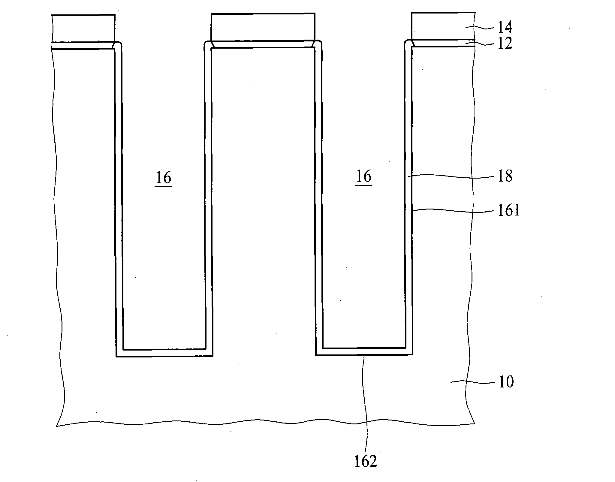
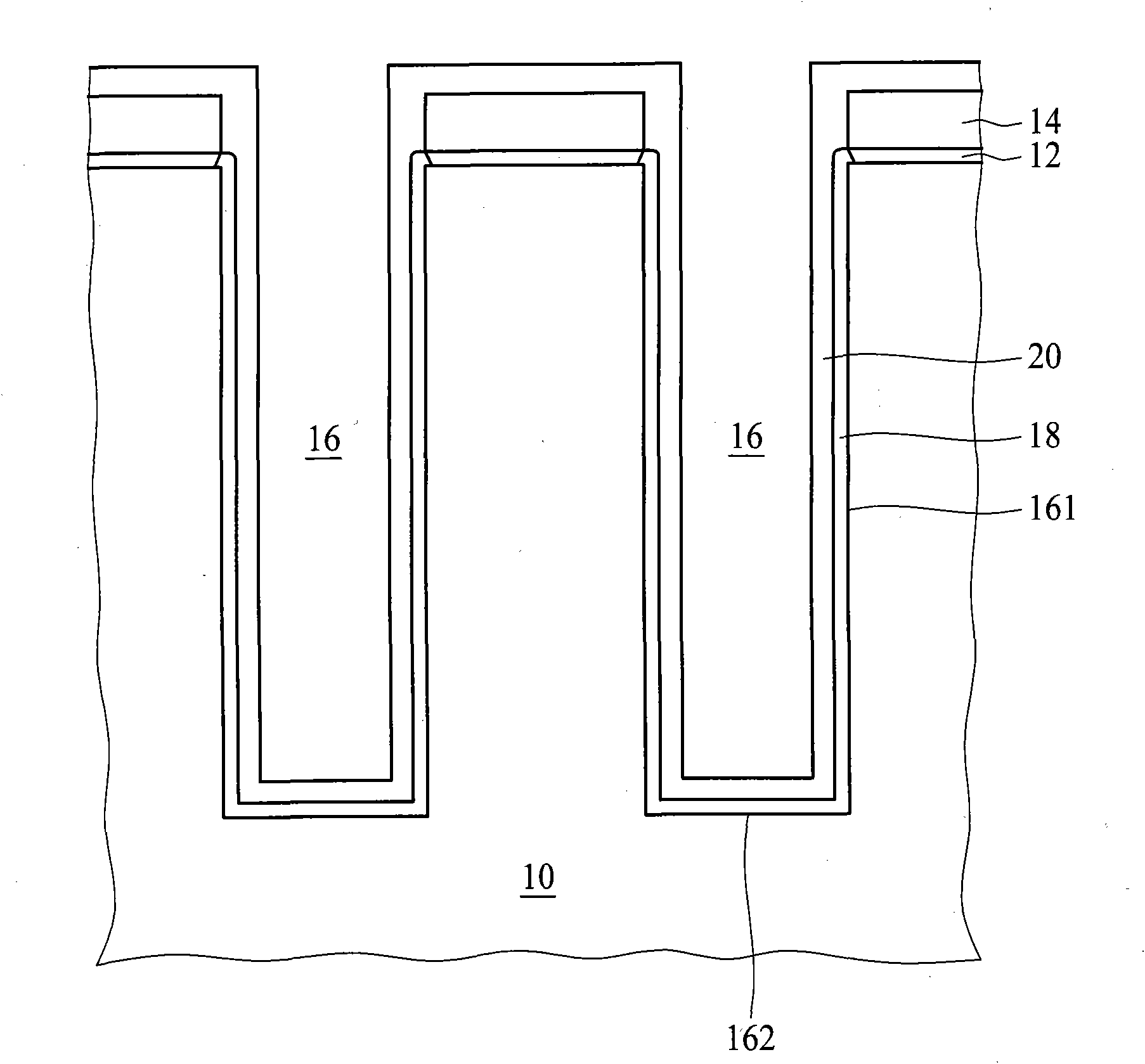
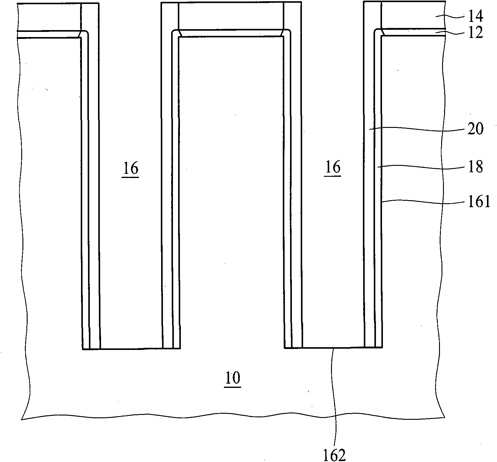
[0030] In one embodiment of the present invention, the dielectric material is first formed on the lower portion of the trench to reduce the filling depth of the trench, so that conventional deposition techniques can be applied to fill the trench. In an embodiment of the present invention, the lower portion of the trench can be filled with a dielectric material or a substance that can be oxidized into a dielectric material. Afterwards, the upper portion of the trench (that is, above the filled dielectric material) can be filled with a spin-on dielectric material or a chemical vapor deposition dielectric material.

[0031] In one embodiment of the present invention, the lower portion of the trench can be filled with epitaxial silicon, which can be converted to silicon oxide in a subsequent thermal oxidation process. In this embodiment, the nitride liner can be formed on the sides of the trench, and the epitaxial silicon can be selectively grown on the bottom of the trench and no...


PUM


Abstract

A semiconductor device includes a substrate and an isolation structure, which includes a trench in the substrate, a lower filling layer at the bottom of the trench, and an upper filling layer on the lower filling layer, wherein the lower filling layer is denser than the upper filling layer, and the lower filling layer contains chlorine. The method for forming an isolation structure includes the steps of forming a trench in a substrate wherein the trench comprises side surfaces and a bottom surface, forming a nitride liner on the side surfaces of the trench, growing an epitaxial silicon layer from to the bottom surface of the trench, oxidizing the epitaxial silicon layer to form a lower filling layer in the lower portion of the trench, and filling a portion of the trench above the lower filling layer with dielectric material.

Description

technical field [0001] The invention relates to a preparation method of an isolation structure and a semiconductor element thereof, in particular to a preparation method of a trench isolation structure using an epitaxy process and an oxidation process and a semiconductor element thereof. Background technique [0002] In order to avoid short circuits caused by mutual interference of electronic components, the known integrated circuit technology generally adopts local oxidation of silicon (LOCOS) or shallow trench isolation (STI) to electrically isolate electronic components on the wafer. Since the field oxide layer formed by the area oxidation method occupies a large area of ​​the wafer and will be accompanied by the formation of a bird's beak phenomenon, the current advanced semiconductor technology mostly uses the shallow trench isolation method to electrically isolate electronic components. [0003] Shallow trench isolation is usually used in CMOS processes below 250nm. S...

Claims


Application Information

Patent Timeline
Patent Type & Authority Applications(China)
IPC IPC(8): H01L21/762H01L29/06
CPCH01L21/76224H01L21/02238
Inventor 陈俊元陈怡荣
Owner NAN YA TECH
Why Eureka
Try Eureka