Shallow groove isolation formation method and semiconductor device manufacturing method

A shallow trench and isolation structure technology, which is applied in semiconductor/solid-state device manufacturing, electrical components, circuits, etc., can solve problems such as latch-up effect, low breakdown, isolation leakage, etc., and achieve good electrical isolation effect

Inactive Publication Date: 2012-10-03
SHANGHAI HUALI MICROELECTRONICS CORP
View PDF4 Cites 2 Cited by
  • Summary
  • Abstract
  • Description
  • Claims
  • Application Information

AI Technical Summary

Problems solved by technology

Poor isolation will cause leakage, low breakdown, latch-up effect, etc.

Method used


Image

  • Shallow groove isolation formation method and semiconductor device manufacturing method
  • Shallow groove isolation formation method and semiconductor device manufacturing method
  • Shallow groove isolation formation method and semiconductor device manufacturing method

Examples


Embodiment Construction

[0023] In order to make the content of the present invention clearer and easier to understand, the content of the present invention will be described in detail below in conjunction with specific embodiments and accompanying drawings.

[0024] Figure 4 to Figure 9 Each step of the method for forming shallow trench isolation according to an embodiment of the present invention is schematically shown.

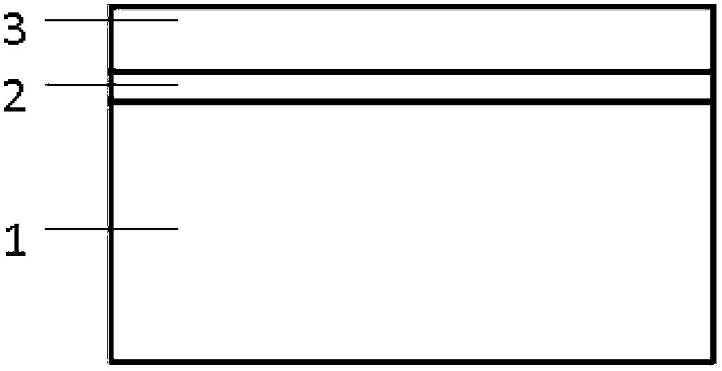
[0025] like Figure 4 As shown, in the shallow trench isolation forming method according to the embodiment of the present invention, first, a silicon oxide layer 2 and a silicon nitride layer 3 are sequentially deposited on a substrate 1;

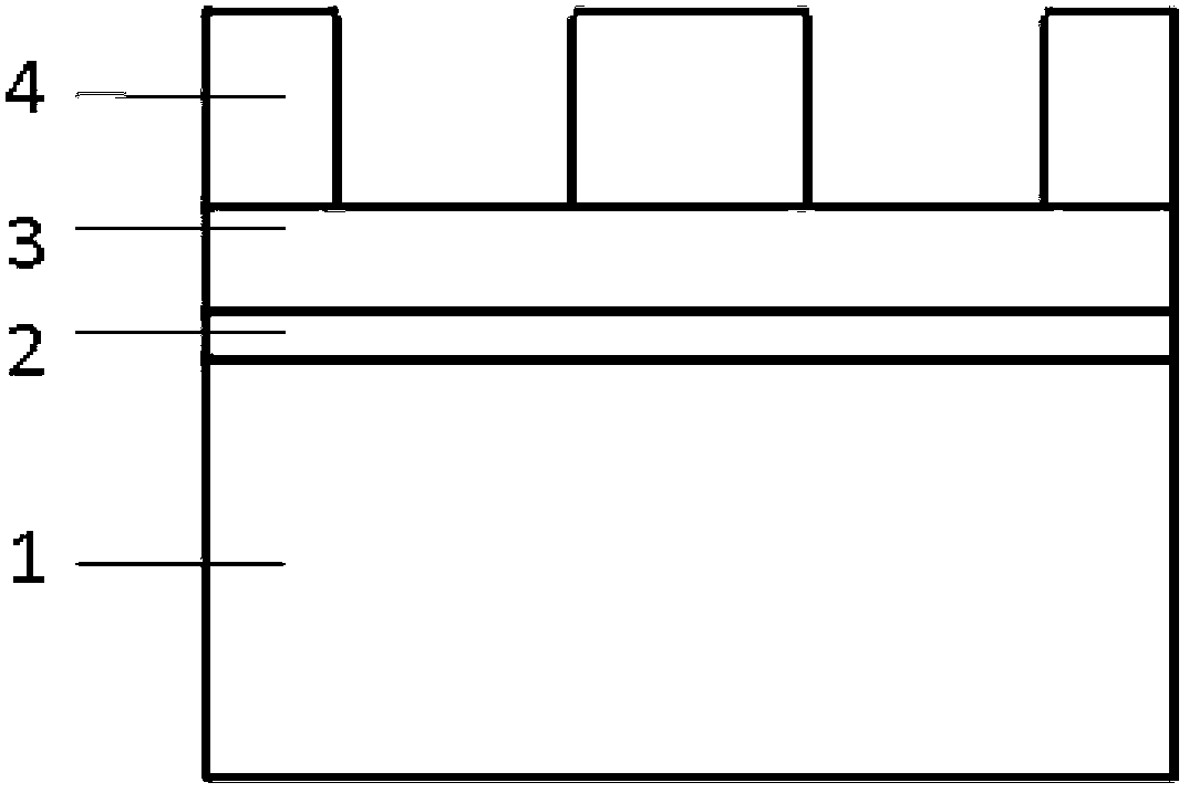
[0026] Then, if Figure 5 As shown, a photoresist layer 4 is arranged on the silicon nitride layer 3 and a pattern of the photoresist layer 4 is formed; specifically, at least a part of the pattern of the photoresist layer 4 corresponds to shallow trench isolation.

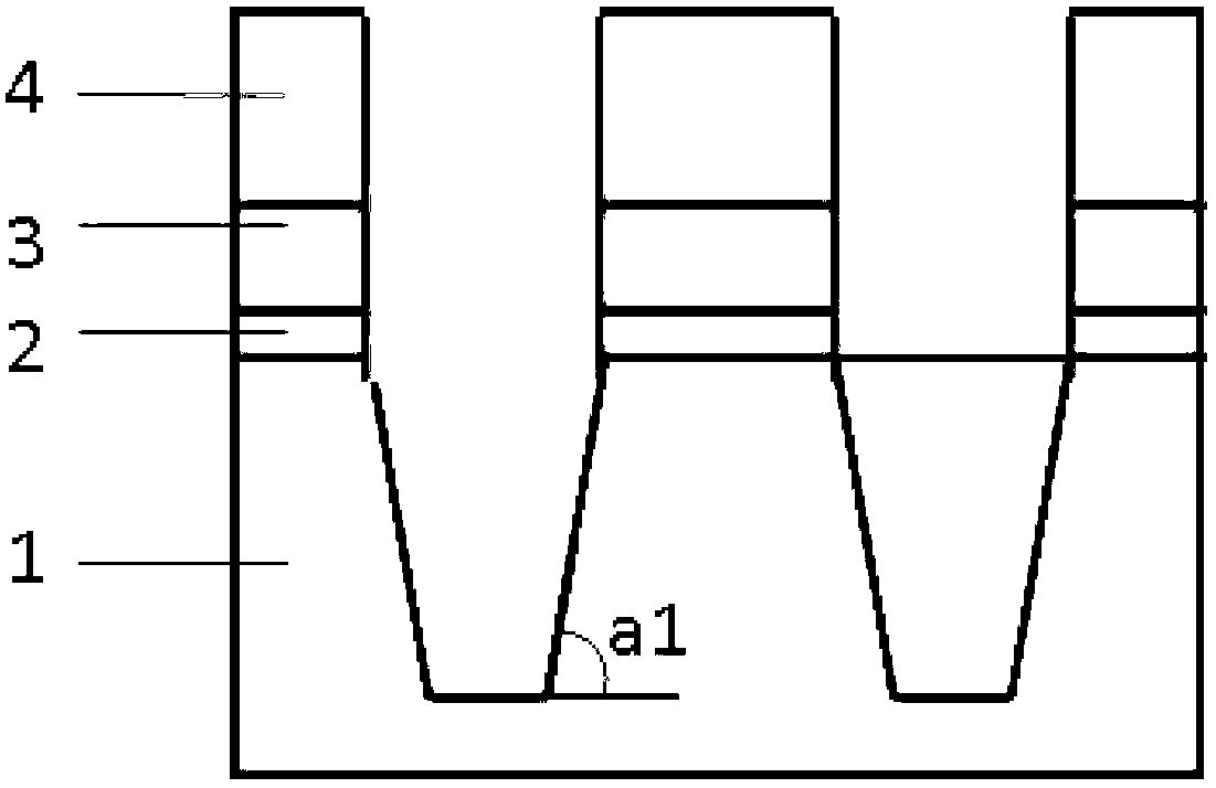
[0027] Thereafter, if Image 6 As shown, an initial shallow trench isolati...


PUM


Abstract

The invention discloses a shallow groove isolation formation method and a semiconductor device manufacturing method. The shallow groove isolation formation method comprises the following steps: depositing a silicon oxide layer and a silicon nitride layer on a substrate; displaying a photoresist layer on the silicon nitride layer so as to form a pattern of the photoresist layer, wherein at least one part of the pattern corresponds to the shallow groove isolation; etching an initial shallow groove isolation structure on the substrate through utilizing patterned photoresist layer; removing the photoresist layer; carrying out angled ion implantation processing to the initial shallow groove isolation structure so as to form an iron implantation area on the side wall of the initial shallow groove isolation structure; performing oxidation treatment to the initial shallow groove isolation structure so as to form an oxidation silicon membrane on the side wall of the initial shallow groove isolation structure; and removing the oxidation silicon membrane so as to form a final shallow groove isolation structure.

Description

technical field [0001] The invention relates to the field of semiconductor manufacturing, and more specifically, the invention relates to a method for forming shallow trench isolation and a method for manufacturing a semiconductor device using the method for forming shallow trench isolation. Background technique [0002] A complete circuit is connected by separate devices through specific electrical pathways. Therefore, in the manufacture of integrated circuits, the devices must be able to be isolated, and these devices must then be able to be interconnected to form the required specific circuit structure. Poor isolation will cause leakage, low breakdown, latch-up effect, etc. Therefore, isolation technology is a key technology in integrated circuit manufacturing. [0003] With the development of devices to deep submicron, due to the stress and bird's beak problems in the traditional local oxidation of silicon (LOCOS) structure, and the field oxygen thinning effect, shallow...

Claims


Application Information

Patent Timeline
Patent Type & Authority Applications(China)
IPC IPC(8): H01L21/762
Inventor 徐强
Owner SHANGHAI HUALI MICROELECTRONICS CORP
Why Eureka
Try Eureka