Method for fabricating silicon wafer solar cell

A technology of solar cells and manufacturing methods, applied in the direction of final product manufacturing, sustainable manufacturing/processing, circuits, etc., to achieve the effects of improving photoelectric conversion efficiency, increasing production rate, and improving production yield

Inactive Publication Date: 2012-05-16
WAKOM SEMICON CORP
View PDF5 Cites 14 Cited by
  • Summary
  • Abstract
  • Description
  • Claims
  • Application Information

AI Technical Summary

Problems solved by technology

In order to reduce production costs, new process technologies and new process equipment are being continuously developed, but their technology maturity and equipment stability still need to be verified and continuously improved

Method used


Image

  • Method for fabricating silicon wafer solar cell
  • Method for fabricating silicon wafer solar cell
  • Method for fabricating silicon wafer solar cell

Examples


Embodiment Construction

[0040] The foregoing and other technical contents, features and effects of the present invention will be clearly presented in the following detailed description of preferred embodiments with accompanying drawings. The directional terms mentioned in the following embodiments, such as: up, down, left, right, front or back, etc., are only directions referring to the attached drawings.

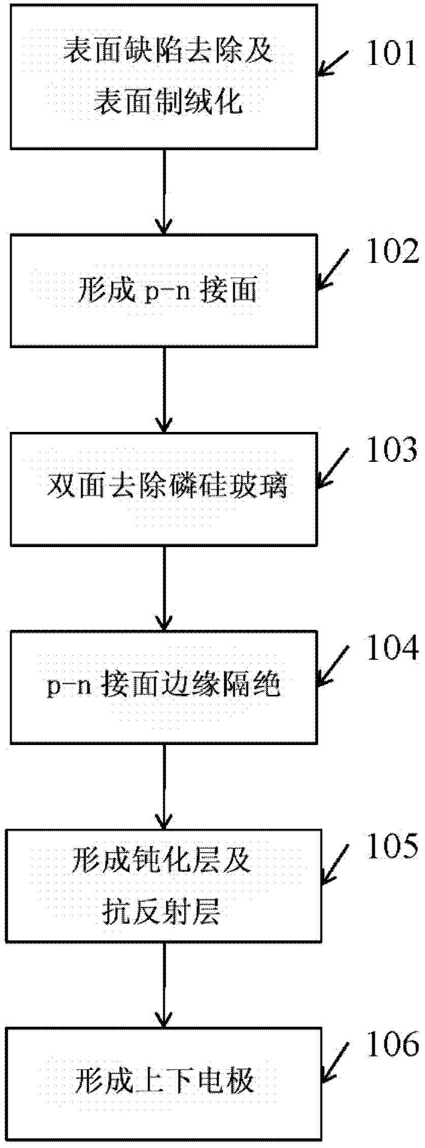
[0041] Traditional general silicon wafer solar cell manufacturing methods, such as figure 1 As shown, the p-n junction edge isolation (Edge Isolation, Edge Isolation) process in step 104 can adopt laser edge isolation (Laser Edge Isolation) technology or wet etching edge isolation technology. In step 104 , the edge isolation technology using the single-side wet etching technology can increase the photoelectric conversion rate by about 0.1% compared with the laser edge isolation technology. In addition, in the traditional single-sided wet etching edge isolation technology, etching a silicon layer ...


PUM

PropertyMeasurementUnit
thicknessaaaaaaaaaa
thicknessaaaaaaaaaa
thicknessaaaaaaaaaa

Abstract

The invention provides a method for fabricating a silicon wafer solar cell, comprising the following steps: texturing a silicon wafer, forming a p-n junction, performing a wet chemical surface treatment, performing a passivation layer formation process, and performing electrodes formation process, wherein the wet chemical surface treatment comprises the following specific process flow: performing a backside phosphosilicate glass (PSG) removal process, performing an edge isolation and backside polish process, performing a double-side phosphosilicate glass and oxide removal process, and performing a front-side shallow junction formation process.

Description

technical field [0001] The present invention relates to a method for manufacturing a solar cell (solar cell), in particular to a wet chemical surface treatment process flow of a method for manufacturing a silicon wafer solar cell. Background technique [0002] Traditional general silicon wafer solar cell manufacturing methods, such as figure 1 In the shown process, a p-type wafer is used as a substrate, and first, defects on the wafer surface are removed and the surface texturization of the wafer is performed (step 101 ). Next, a p-n junction is formed (step 102 ), that is, an n-type emitter layer with a uniform surface is formed by high-temperature phosphorus diffusion. Then, a wet chemical process is performed to remove the surface phosphosilicate glass (Phosphosilicate Glass; PSG) (step 103), because during the phosphorus diffusion (POCl3 doping & diffusion) process in the high-temperature furnace tube, the reaction of POCl3 and silicon will be on the wafer surface An i...

Claims


Application Information

Patent Timeline
Patent Type & Authority Applications(China)
IPC IPC(8): H01L31/18
CPCH01L31/068H01L31/1804Y02E10/547Y02P70/50
Inventor 钱家锜谢日舜林育玫
Owner WAKOM SEMICON CORP
Why Eureka
Try Eureka