

Thin film transistor and method for manufacturing thin film transistor
A technology for thin film transistors and sintered bodies, which is applied in the manufacture of transistors, semiconductor/solid-state devices, semiconductor devices, etc., can solve the problems that the characteristics of TFT devices are difficult to become stable, it is difficult to obtain the characteristics of TFT devices, and the transmission characteristics are changed, and the cost is low. , high reliability, high productivity
- Summary
- Abstract
- Description
- Claims
- Application Information
AI Technical Summary
Problems solved by technology
Method used
Image

Examples
Embodiment 1 to 3
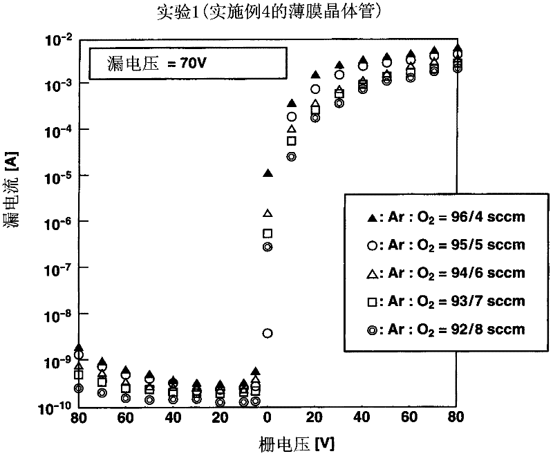
[0112] Examples 1 to 3, Comparative Example 1
[0113] [Performance test of semiconductor film]
[0114] First, the In-W-Zn-O film, the In-W-Sn-O film, and the In-W-Sn-Zn film used as the channel layer in the thin film transistor belonging to the first invention of the present invention were evaluated in the following manner - Properties of O films.
[0115] Sample preparation
[0116] (Sample 1: In-W-Zn-O film)
[0117] On a 1.1 mm thick quartz glass substrate cleaned with ethanol and acetone, a 30 nm thick In-W-Zn-O film was formed by DC magnetron sputtering without heating the substrate. The sputtering conditions were as follows.
[0118] (sputtering condition)
[0119]
[0120] From the quartz glass substrate on which the In-W-Zn-O film was thus formed, a test piece of 10 mm x 10 mm was formed by dicing. A shadow mask was attached to the test piece in such a manner as to hide the central portion of the test piece, and ohmic electrodes composed of a 30 nm-thick I...
Embodiment 1
[0145] A thermal oxide film (SiO 2 , 300 nm thick) on a silicon wafer, a 30 nm thick In-W-Zn-O film was formed as a channel layer by DC magnetron sputtering. In this case, the sputtering conditions were set to be the same as in the case of forming the In—W—Zn—O film of Sample 1 described above, and the sputtering was performed without heating the substrate.
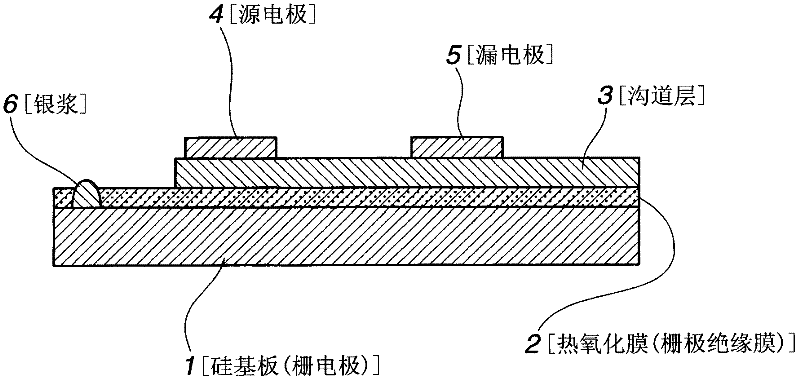
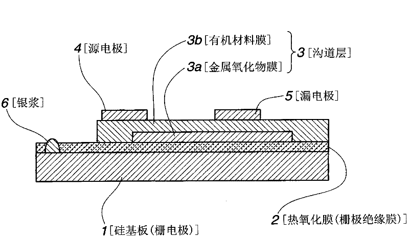
[0146] On the channel layer obtained as above, a 30 nm thick ITO film as source and drain electrodes was formed by DC magnetron sputtering process to fabricate as figure 1 A thin film transistor (TFT device) constructed as shown. In this case, the sputtering conditions were set to be the same as in the case of forming the ohmic electrode of Sample 1 described above. In forming the source and drain electrodes, patterning was performed using a shadow mask to obtain a channel length of 0.1 mm and a channel width of 6.4 mm.
Embodiment 2
[0148] A thermal oxide film (SiO 2 , 300 nm thick) on a silicon wafer, a 30 nm thick In-W-Sn-O film was formed as a channel layer by DC magnetron sputtering. In this case, the sputtering conditions were set to be the same as in the case of forming the In—W—Sn—O film of Sample 2 described above, and sputtering was performed without heating the substrate.
[0149] On the channel layer thus obtained, a 30 nm-thick ITO film was formed as a source electrode and a drain electrode by DC magnetron sputtering treatment to fabricate as figure 1 A thin film transistor (TFT device) constructed as shown. In this case, the sputtering conditions were set to be the same as in the case of forming the ohmic electrode of Sample 2 described above. In forming the source and drain electrodes, patterning was performed using a shadow mask in the same manner as in Example 1 above to obtain a channel length of 0.1 mm and a channel width of 6.4 mm.
PUM
 Abstract
Description
Claims
Application Information