Semiconductor memory cell, device and preparation method thereof

A storage unit and semiconductor technology, applied in the field of microelectronics, can solve the problems of short data retention time of FBC, and achieve the effects of high-density three-dimensional process integration, improvement of retention characteristics, and reduction of refresh times

Active Publication Date: 2012-05-23
INST OF MICROELECTRONICS CHINESE ACAD OF SCI
View PDF4 Cites 4 Cited by
  • Summary
  • Abstract
  • Description
  • Claims
  • Application Information

AI Technical Summary

Problems solved by technology

[0008] The purpose of the present invention is to solve the problem that the holes stored near the substrate can easily leak out through the PN junction between the source region and the substrate or the PN junction between the drain region and the substrate when the floating body memory unit in the prior art is powered off. , thus leading to the technical problem of the short data retention time of FBC, thereby providing a semiconductor memory unit, a device and a preparation method thereof

Method used


Image

  • Semiconductor memory cell, device and preparation method thereof
  • Semiconductor memory cell, device and preparation method thereof
  • Semiconductor memory cell, device and preparation method thereof

Examples


Embodiment 1

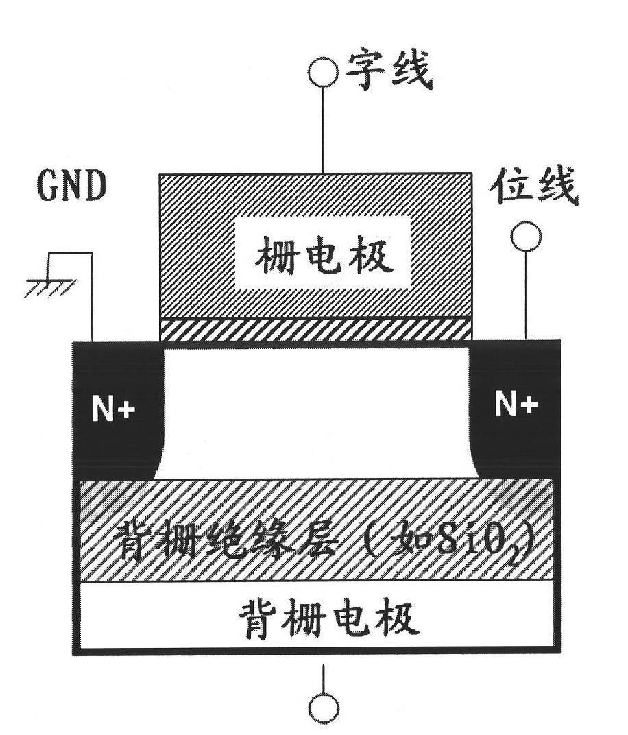
[0024] image 3 It is a schematic diagram of a semiconductor memory unit according to an embodiment of the present invention. Such as image 3 As shown, the semiconductor memory unit includes: a substrate; a channel region above the substrate; a gate region above the channel region; above the substrate, gate regions on both sides of the channel region a source region and a drain region; a buried layer located between the substrate and the channel region and made of a material whose forbidden band width is narrower than that of the channel region material.

[0025] In this embodiment, the material of the channel region is Si or stressed silicon, and the material of the buried layer is a group IV material or a III-V group material, such as Si x Ge 1-x , Ge, GaN, or InP; or the material of the channel region is Si x Ge 1-x , the material of the buried layer is Ge.

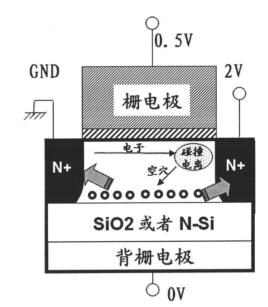
[0026] Since the forbidden band width of the buried layer is narrower than that of the material of the channe...

Embodiment 2

[0028] This embodiment will further optimize the technical solution on the basis of the first embodiment.

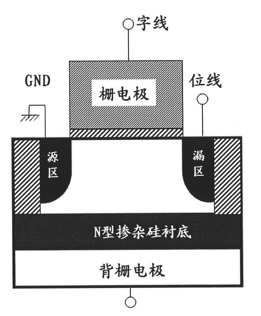
[0029] Figure 4 It is a schematic diagram of a semiconductor memory unit according to Embodiment 2 of the present invention. Such as Figure 4 In the shown semiconductor memory unit, an insulating layer is further included between the source / drain region and the substrate, on both sides of the buried layer. Preferably, the insulating layer is partially located between the channel region and the substrate. The material of the insulating layer is one of the following materials: Ge x o y , SiO 2 , SiC, Si x N y . The insulating layer can effectively reduce the area of ​​the PN junction, thereby effectively reducing the leakage current of the PN junction from the substrate to the source region and from the substrate to the drain region.

[0030] Figure 5 For the second embodiment of the present invention, the semiconductor storage unit is Figure 4 Schematic dia...

Embodiment 3

[0034] This embodiment provides a semiconductor storage device, which may include one or more semiconductor storage units disclosed in Embodiment 2 or Embodiment 2, and obtain corresponding technical effects.


PUM


Abstract

The invention discloses a semiconductor memory cell, a device and a preparation method thereof. The semiconductor memory cell comprises: a substrate, a channel region located above the substrate, a grid region located above the channel region, a source area and leakage area located above the substrate and on two sides of the channel region, a buried layer located between the substrate and the channel region and is made by a material whose forbidden bandwidth is narrower than the forbidden bandwidth of the channel region material. Because the forbidden bandwidth of the buried layer is narrower than the forbidden bandwidth of the channel region material, a hole barrier is formed in the buried layer so that the hole stored in the buried layer is difficult to be leaked out facing the barrier. By using the method of the invention, information maintaining time of the memory cell using a floating body effect can be increased.

Description

technical field [0001] The invention relates to the technical field of microelectronics, in particular to a semiconductor storage unit, a device and a preparation method thereof. Background technique [0002] Microelectronics products are mainly divided into two categories: logic devices and memory devices. As an important part of storage devices, dynamic random access memory (DRAM) can provide high-speed data read and write operations, but the stored information is easily lost in the event of power failure, so it is called volatile semiconductor memory. In computer systems, DRAMs are generally placed between high-speed microprocessors and low-speed non-volatile memories, and are used to match high-speed data processing and low-speed data access. With the continuous development of information technology, the development of high-speed and high-density DRAM has become an important direction of storage technology research. [0003] A traditional dynamic random access memory d...

Claims


Application Information

Patent Timeline
Patent Type & Authority Applications(China)
IPC IPC(8): H01L27/108H01L21/8242H01L21/762G11C11/401
CPCH01L29/7841Y10S438/933Y10S438/938
Inventor 霍宗亮刘明
Owner INST OF MICROELECTRONICS CHINESE ACAD OF SCI
Why Eureka
Try Eureka