Method for depositing semiconductor film on flexible substrate

A flexible substrate and semiconductor technology, applied in semiconductor devices, climate sustainability, liquid chemical plating, etc., can solve the problems of inability to achieve semiconductor film deposition, insufficient utilization of reaction solutions, and high cost of semiconductor films, and achieve a simple structure. , Low manufacturing cost, good uniformity

Inactive Publication Date: 2012-05-30
CHINA ELECTRONIC TECH GRP CORP NO 18 RES INST
View PDF6 Cites 2 Cited by
  • Summary
  • Abstract
  • Description
  • Claims
  • Application Information

AI Technical Summary

Problems solved by technology

[0003] Existing chemical bath devices for preparing semiconductor thin films are mostly used on rigid substrates such as glass, and cannot deposit semiconductor thin films on rolls of flexible substrates
However, the devices for preparing semiconductor thin films on flexible substrates are mostly roll-to-roll designs, the equipment structure is complex, the reaction solution is not fully utilized, and the uniformity of deposited films on moving substrates is poor. Large-scale deposition of semiconductor thin films on flexible substrates very high cost

Method used


Image

  • Method for depositing semiconductor film on flexible substrate
  • Method for depositing semiconductor film on flexible substrate

Examples


Embodiment

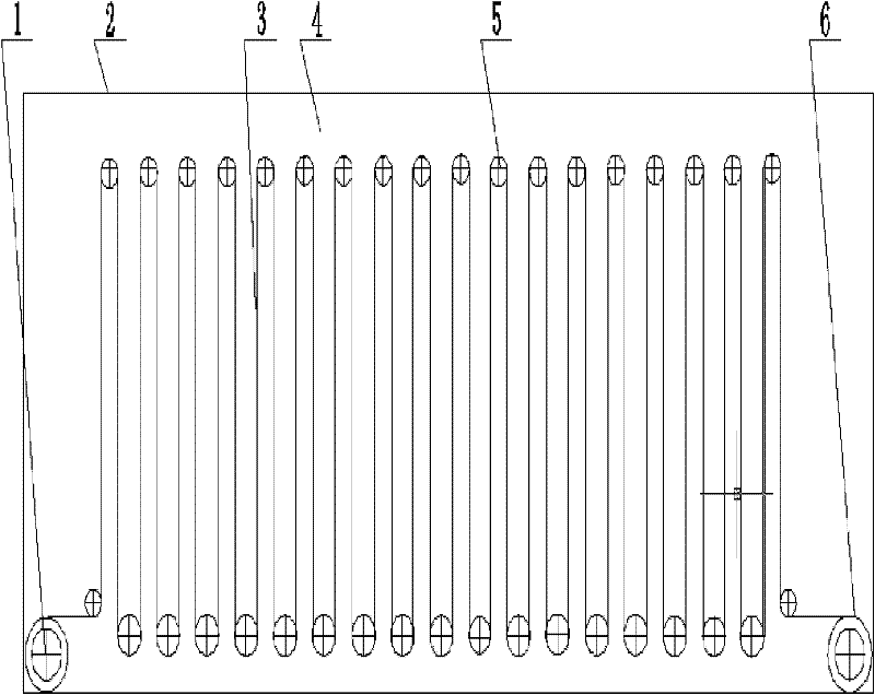
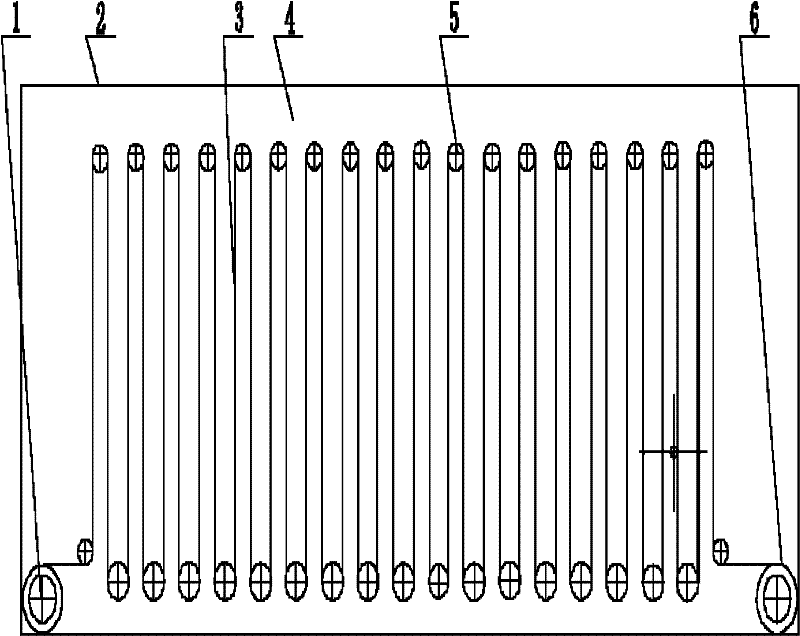
[0020] Embodiment: refer to attached figure 1 . Polypropylene plastic is poured on the stainless steel plate as the material for preparing the reaction tank 2. According to the size requirements, a rectangular plate is cut out as the reaction tank bottom plate 4, and four side panels and reaction tanks corresponding to the size of the reaction tank bottom plate Upper cover; a hole is drilled on both sides of the polypropylene plastic surface of the bottom plate of the reaction tank near the length direction, for installing the reel 1 with the motor and the reel 6 without the motor; the bottom plate of the reaction tank is close to the length direction A row of holes with the same hole spacing are drilled at both ends of each of the two ends, and are used to install the fixed shaft 5 used to support the flexible substrate. horn.

[0021] A smooth fixed shaft whose length is greater than the width of the flexible substrate is made of polypropylene plastic, and the fixed shaft ...


PUM


Abstract

The invention relates to a method for depositing a semiconductor film on a flexible substrate, which comprises the following steps: (1) preparing a reaction tank material; (2) mounting a part on a reaction tank base plate; (3) fixedly mounting four side plates around the reaction tank base plate to form a case body; (4) mounting a flexible substrate; (5) transferring the flexible substrate which is completely soaked in a reaction solution from one scroll to another scroll so as to allow the end surface of the flexible substrate to be snake-shaped. According to the invention, the flexible substrate is winded into a fixed shaft with a snake-shaped end surface; the scroll is driven by a motor, and the flexible substrate is transferred from one scroll to another scroll through snake-shaped movement in the reaction solution; thereby the substrate disposed in the reaction tank is as long as possible; the deposition area of the substrate is effectively increased; the reaction solution is made full use of; the flexible substrate is deposited completely in the reaction solution so as to form a semiconductor film with good uniformity; the device has a simple structure; the manufacturing cost is low; and the method has the characteristic of large-scale production.

Description

technical field [0001] The invention belongs to the technical field of devices for manufacturing semiconductor thin films, in particular to a method for depositing semiconductor thin films on a flexible substrate. Background technique [0002] CdS thin film, ZnS thin film, CdTe thin film, In2S3 thin film, Cu InS2 thin film, CuInSe2 thin film, Cu2S thin film and other thin films are widely used in semiconductor devices such as thin film solar cells. For example, CdTe thin film, CuInS2 thin film, CuInSe2 thin film, Cu2S thin film can be used as the absorbing layer of solar cells, which can absorb photons and convert them into photogenerated carriers; while CdS thin films, ZnS thin films, and In2S3 thin films can be used as n-type layers or The buffer layer. The methods used to prepare these thin films are: vacuum evaporation method, sputtering method, molecular beam epitaxy, chemical bath, etc. The first three methods generally require high temperature and high pressure, so ...

Claims


Application Information

Patent Timeline
Patent Type & Authority Applications(China)
IPC IPC(8): C23C18/00H01L31/18
CPCY02P70/50
Inventor 李微李巍赵彦民冯金辉杨立乔在祥刘兴江
Owner CHINA ELECTRONIC TECH GRP CORP NO 18 RES INST
Why Eureka
Try Eureka