Transistor and manufacturing method for same

A manufacturing method and transistor technology, applied in semiconductor/solid-state device manufacturing, semiconductor devices, electrical components, etc., can solve the problems of obvious short-channel effect of transistors and unsatisfactory device performance, etc., to improve short-channel effect and improve performance , The effect of reducing the junction leakage current

Active Publication Date: 2014-01-08
SEMICONDUCTOR MANUFACTURING INTERNATIONAL (BEIJING) CORP
View PDF3 Cites 0 Cited by
  • Summary
  • Abstract
  • Description
  • Claims
  • Application Information

AI Technical Summary

Problems solved by technology

[0009] In practice, it is found that the short channel effect of the transistor fabricated by the existing method is obvious, and the performance of the device is not ideal

Method used


Image

  • Transistor and manufacturing method for same
  • Transistor and manufacturing method for same
  • Transistor and manufacturing method for same

Examples


Embodiment Construction

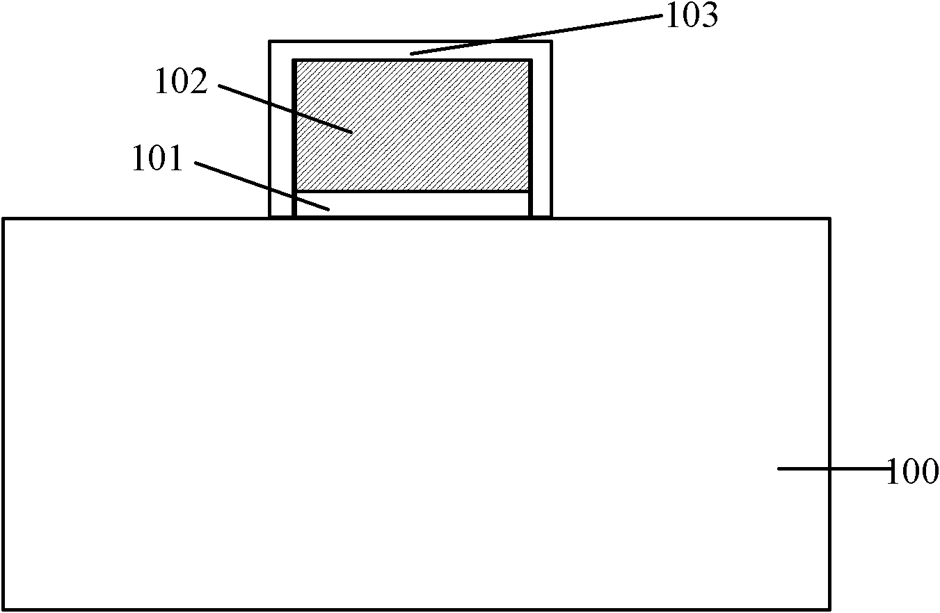
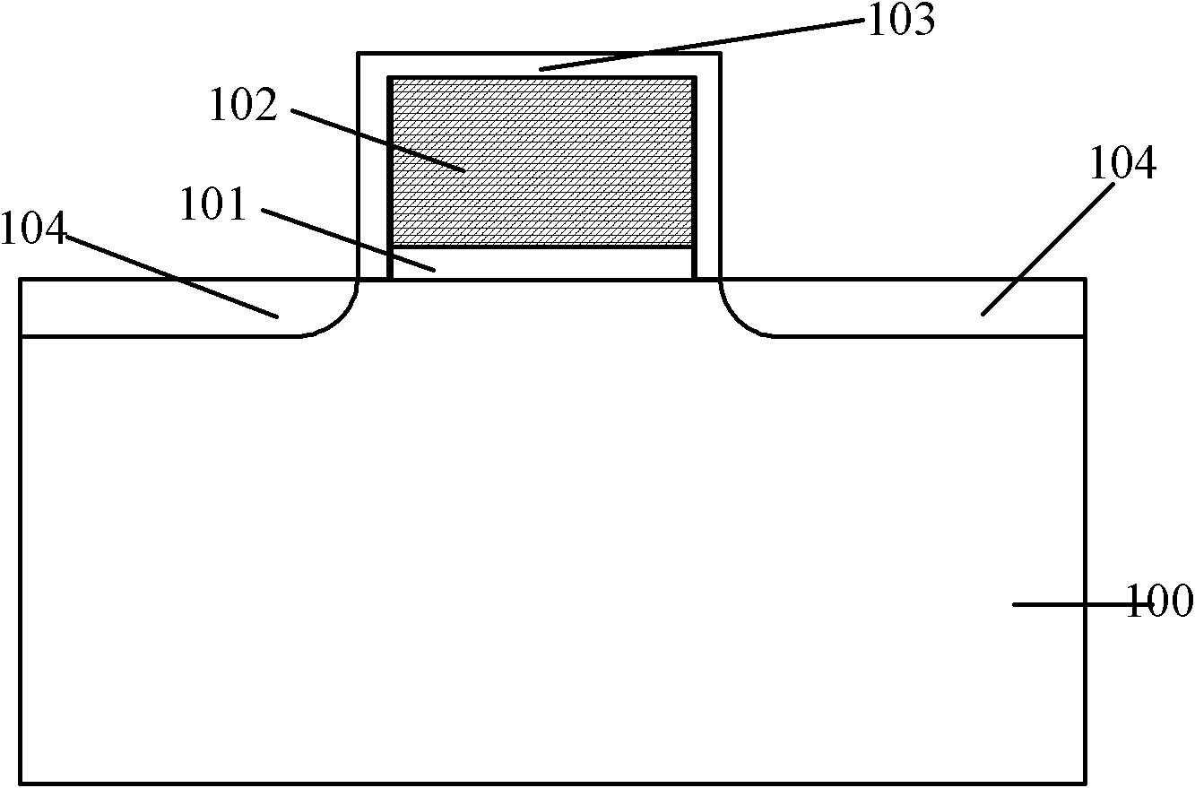
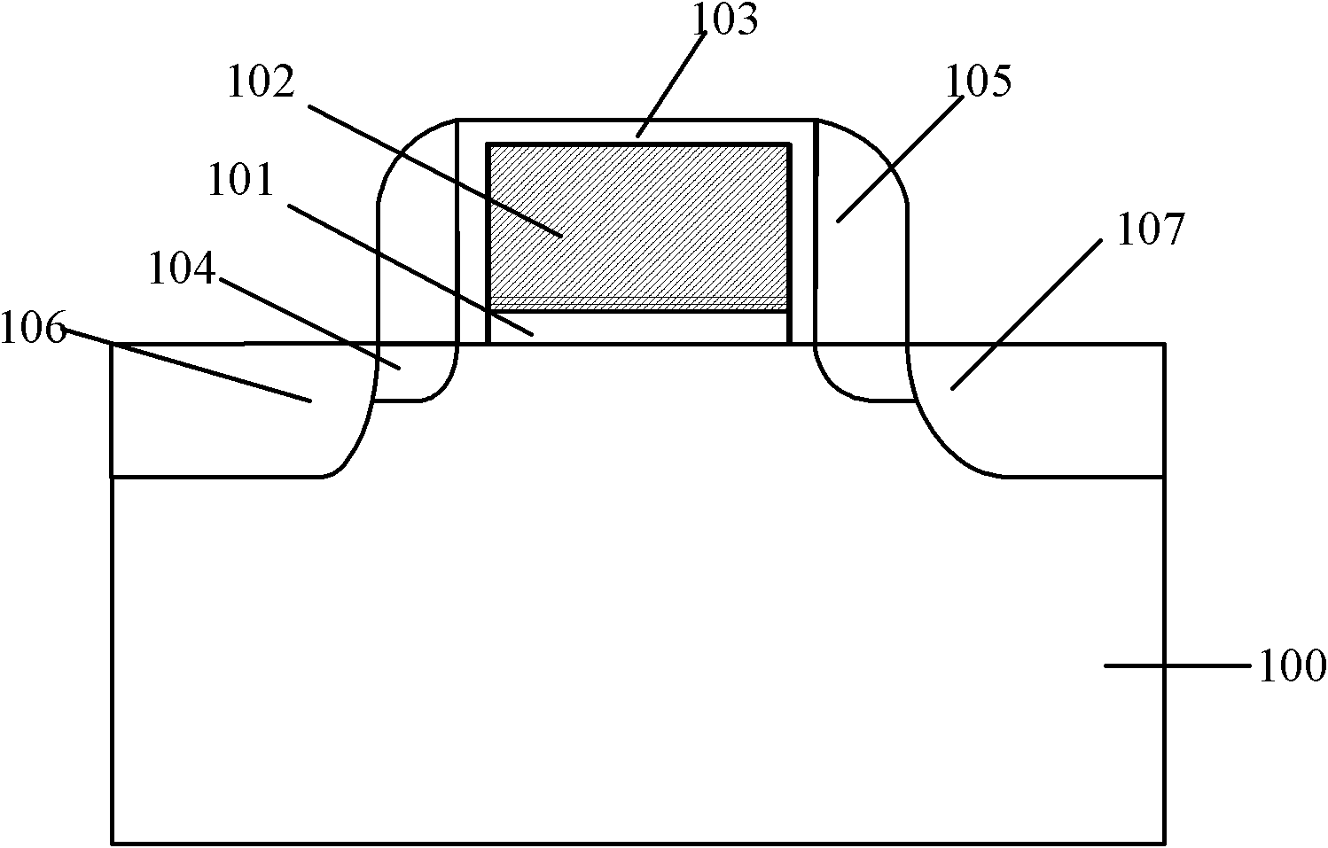
[0053] The short channel effect of the transistor manufactured by the existing method is obvious, and the performance of the device is not ideal. With the development of semiconductor technology, ultra-shallow junction technology is applied to make the source region and the drain region, and the ion lateral diffusion between the source region and the drain region is more serious, which makes the short channel effect more obvious, and the source region and the drain region There is a large junction capacitance and junction leakage current between the drain region and the semiconductor substrate, which reduces the response speed of the device and affects the performance of the device.

[0054] In order to solve the above problems, the inventor proposes a method for making a transistor, please refer to Figure 4 The schematic flow chart of the transistor manufacturing method of the present invention shown, the method includes:

[0055] Step S1, providing a semiconductor substrat...


PUM


Abstract

The invention provides a transistor and a manufacturing method for the same. The method includes the steps: providing a semiconductor substrate with a formed active layer; forming buried layers spaced from the active layer on the surface of the semiconductor substrate on two sides of the active layer; forming first epitaxial layers flush with the active layer on the surfaces of the buried layers and in the space between each buried layer and the active layer; forming grooves exposed out of the semiconductor substrate in the first epitaxial layers, wherein the grooves are positioned among the buried layers and the active layer; forming buried side walls in the grooves, wherein the thickness of each buried side wall is smaller than the depth of each groove; forming second epitaxial layers on the surfaces of the buried side walls, the active layer and the first epitaxial layers; forming gate structures on the surfaces of the second epitaxial layers above the active layer; and forming a source region and a drain region in the second epitaxial layer and the first epitaxial layer on two sides of each gate structure, wherein the source region and the drain region are positioned on two sides of an isolating side wall. By the aid of the method, the short-channel effect and the performance of the transistor are improved.

Description

technical field [0001] The invention relates to the field of semiconductors, in particular to a transistor and a manufacturing method thereof. Background technique [0002] Metal-oxide-semiconductor (MOS) transistors are the most basic devices in semiconductor manufacturing. They are widely used in various integrated circuits. According to the main carrier and the type of doping during manufacturing, they are divided into NMOS and PMOS transistors. [0003] The prior art provides a method for manufacturing a transistor. Please refer to Figure 1 to Figure 3 , is a schematic cross-sectional structure diagram of a fabrication method of a transistor in the prior art. [0004] Please refer to figure 1 A semiconductor substrate 100 is provided, on which a gate dielectric layer 101 and a gate 102 are formed, and the gate dielectric layer 101 and the gate 102 form a gate structure. [0005] continue to refer figure 1 , performing an oxidation process to form an oxide layer 10...

Claims


Application Information

Patent Timeline
Patent Type & Authority Patents(China)
IPC IPC(8): H01L21/336H01L29/78H01L29/12H01L29/06
Inventor 赵猛韩永召
Owner SEMICONDUCTOR MANUFACTURING INTERNATIONAL (BEIJING) CORP
Why Eureka
Try Eureka