Semiconductor device
A semiconductor and device technology, applied in the field of semiconductor devices, can solve the problem that the P-type region is difficult to absorb holes, etc.
- Summary
- Abstract
- Description
- Claims
- Application Information
AI Technical Summary
Problems solved by technology
Method used
Image

Examples
no. 1 example
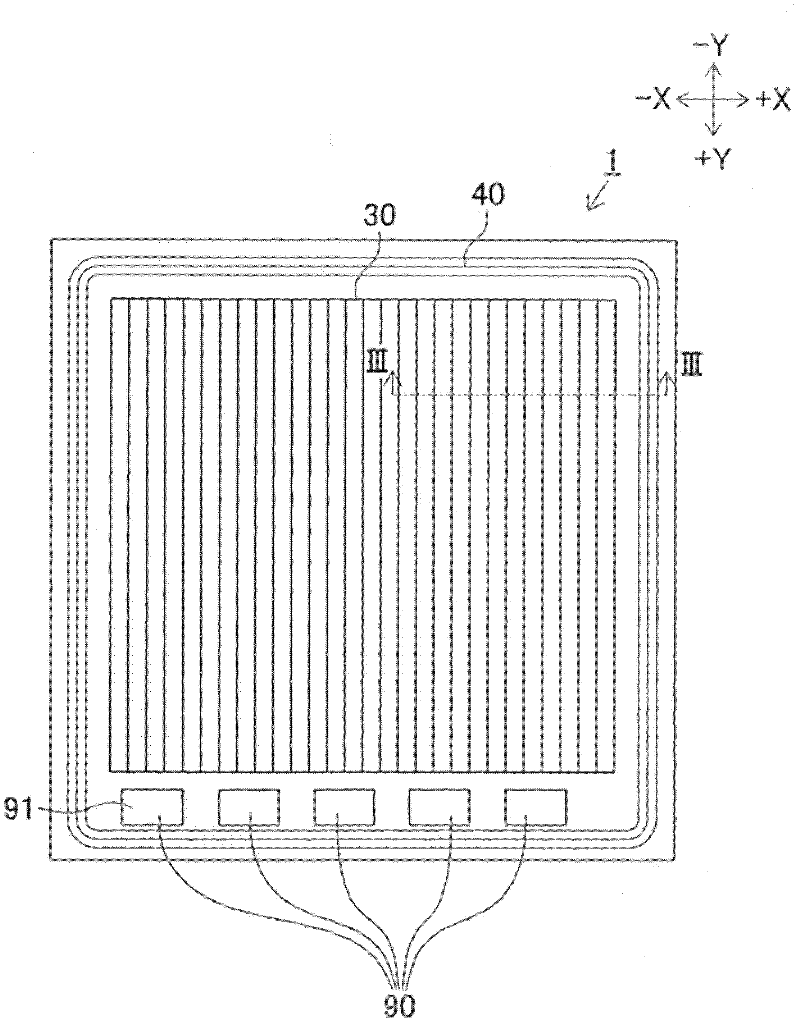
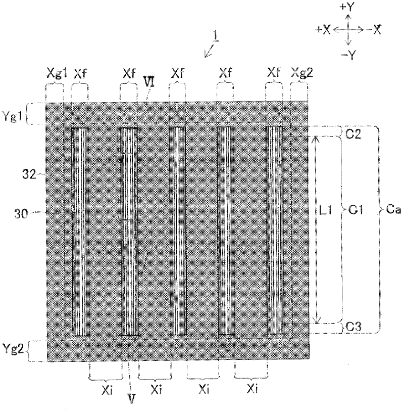
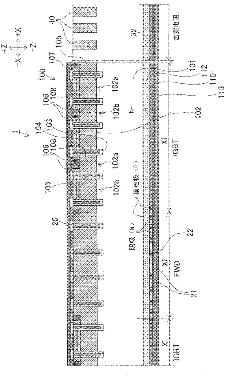
[0042] The following reference Figure 1-7D A semiconductor device 1 according to a first embodiment of the present invention is described. figure 1 is a diagram showing a front side view of the semiconductor device 1 . figure 2 is a diagram showing a rear side view of the semiconductor device 1 . image 3is shown along figure 1 A diagram of a cross-sectional view taken along line III-III. Figure 4A is a diagram showing a cross-sectional view of an IGBT element of the semiconductor device 1 . Figure 4B is a diagram showing a cross-sectional view of a diode element of the semiconductor device 1 . Figure 5 yes figure 2 Diagram of an enlarged view of part V in . Figure 6 is showing figure 2 Diagram of an enlarged view of part V1 in . Figures 7A-7D is a diagram illustrating a method of manufacturing the semiconductor device 1 .
[0043] Such as image 3 As shown in , according to the first embodiment, a semiconductor device 1 includes a trench gate field stop (FS...
no. 2 example
[0115] The following reference Figure 13 and 14 A semiconductor device 200 according to a second embodiment of the present invention is described. Figure 13 is a diagram showing a cross-sectional view of the semiconductor device 200 . Figure 14 is a diagram showing a rear side view of the semiconductor device 200 . Note that for simplicity, the Figure 14 The cathode electrode 202 is omitted.
[0116] The semiconductor device 200 is configured as a diode. on silicon substrates such as N - An anode electrode (ie, a first electrode) 201 is formed on the front surface side of a type semiconductor substrate 210 . A cathode electrode (ie, a second electrode) 202 is formed on the rear surface side of the semiconductor substrate 210 . Specifically, the anode electrode 201 is connected to the anode region (ie, the first semiconductor region) 204, which will be described later. The cathode electrode 202 is connected to the cathode region formed by the cathode side N of the s...
no. 3 example
[0152] The following reference Figure 19A , 19B and 20A describe a semiconductor device 300 according to a third embodiment of the present invention. Figure 19A is a diagram showing a front side view of the semiconductor device 300 . Figure 19B is shown taken along a line extending in the width direction Figure 19A An illustration of a partial cross-sectional view of . Figure 20A is a diagram showing a rear side view of the semiconductor device 300 .
[0153] as in Figure 19A As shown in , the semiconductor device 300 has a rectangular plan shape. The semiconductor device 300 is configured as a double diffused MOS (DMOS) transistor. The semiconductor device 300 includes a silicon substrate such as N - Type semiconductor substrate 301. The semiconductor substrate 301 has a front surface and a rear surface opposite to the front surface. A plurality of DMOS elements 320 are arranged in an element region 330 of a semiconductor substrate 301 . The element region 330...
PUM
 Abstract
Description
Claims
Application Information
 - R&D
- Intellectual Property
- Life Sciences
- Materials
- Tech Scout
- Unparalleled Data Quality
- Higher Quality Content
- 60% Fewer Hallucinations
Browse by: Latest US Patents, China's latest patents, Technical Efficacy Thesaurus, Application Domain, Technology Topic, Popular Technical Reports.
© 2025 PatSnap. All rights reserved.Legal|Privacy policy|Modern Slavery Act Transparency Statement|Sitemap|About US| Contact US: help@patsnap.com