Supercharge Your Innovation With Domain-Expert AI Agents!

Optical proximity correction method of covered shape

A technology of optical proximity effect and topography, which is applied in the photo-engraving process of optics, pattern surface, and originals for opto-mechanical processing, etc. The actual value of the size becomes smaller, etc., to achieve the effect of improving the coverage capacity

Active Publication Date: 2012-06-06
SHANGHAI HUAHONG GRACE SEMICON MFG CORP
View PDF6 Cites 3 Cited by
  • Summary
  • Abstract
  • Description
  • Claims
  • Application Information

AI Technical Summary

Problems solved by technology

[0005] Therefore, the defect of adopting the optical proximity effect correction method of the existing coverage topography is that when the photolithography size of each front layer line pattern of the current layer etching pattern changes, the coverage ability of the current layer photoresist pattern to the front layer etching pattern will be reduced. become worse, and cannot effectively control the coverage size B corresponding to the lithography size of different front-layer line patterns, which will make the actual value of part of the coverage size B smaller. When the coverage size B is smaller than a certain value, it will affect the subsequent The photolithographic process and electrical performance of the circuit

Method used


Image

  • Optical proximity correction method of covered shape
  • Optical proximity correction method of covered shape
  • Optical proximity correction method of covered shape

Examples


Embodiment Construction

[0021] Such as image 3 As shown, the flow chart of the method for correcting the optical proximity effect of the coverage topography of the present invention is shown. The method for correcting the optical proximity effect of the overlay topography according to the embodiment of the present invention includes the following steps:

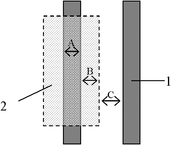
[0022] Step 1, such as figure 1 As shown, a group of test patterns are designed according to the existing optical proximity effect correction method, including the design on the front layer mask, the design on the current layer mask, and the interaction between the design on the current layer mask and the design on the front layer mask. Overlap; through the design on the front mask plate, the front layer etching pattern is formed on the flat sheet, that is, only different film layers, but no lower layer graphics, through the design on the current layer mask plate, the The design on the mask plate of the current layer and the design on the mask pl...


PUM


Abstract

The invention discloses an optical proximity correction method of a covered shape. The method comprises steps that: a set of detection patterns are designed; each covering dimension measured value of a current-layer photoresist patterns upon a previous-layer etching patterns is measured; according to the covering dimension measured values, and with a photo-etching technology and electrical properties, covering dimension specification values of the current-layer photoresist patterns upon the previous-layer etching patterns are obtained; according to the covering dimension specification values, photo-etching dimensions of the line patterns on the current layer is adjusted, such that the covering dimensions of the current-layer line patterns covering the previous-layer line patterns with different photo-etching dimensions are no smaller than the covering dimension specification values. With the method provided by the invention, the covering capacity of the current-layer photoresist patterns upon the previous-layer etching patterns is improved; it is effectively ensured that the covering dimensions corresponding to the previous-layer etching line patterns with different dimensions are larger than the covering dimension specification values. Therefore, the subsequent photo-etching technology and the electrical properties can satisfy the requirements of technologies.

Description

technical field [0001] The invention relates to a semiconductor integrated circuit manufacturing process method, in particular to an optical proximity effect correction method for covering topography. Background technique [0002] In the existing Optical Proximity Correction (OPC) method, for the accuracy of OPC modeling, the modeling will be carried out through the graphic data collected on the flat sheet. The flat sheet refers to only different film layers, but no The silicon chip of the underlying pattern, that is, the silicon chip only has a flat film structure and does not have a stepped pattern structure. However, the silicon wafers of general products often include the underlying graphics structure, and the existing OPC method cannot reflect the impact of the underlying graphics' morphology on OPC modeling, so the OPC model itself lacks the underlying graphics' morphology. technical coverage. [0003] Such as figure 1 As shown, it is a top view structure diagram of...

Claims


Application Information

Patent Timeline
Patent Type & Authority Applications(China)
IPC IPC(8): G03F1/36
Inventor 陈福成阚欢
Owner SHANGHAI HUAHONG GRACE SEMICON MFG CORP
Features
  • R&D
  • Intellectual Property
  • Life Sciences
  • Materials
  • Tech Scout
  • Unparalleled Data Quality
  • Higher Quality Content
  • 60% Fewer Hallucinations
Learn More