Method and loading plate for degumming cleaning silicon wafer

A technology for degumming silicon wafers and loading plates, which is applied in cleaning methods and utensils, cleaning methods using liquids, chemical instruments and methods, etc., and can solve the problems of poor cleaning effect, inability to separate silicon wafers, and low production efficiency. The effect of improving labor productivity, shortening cleaning time, and lowering manufacturing costs

Inactive Publication Date: 2012-06-06
TIANWEI NEW ENERGY HLDG +1
View PDF5 Cites 6 Cited by
  • Summary
  • Abstract
  • Description
  • Claims
  • Application Information

AI Technical Summary

Problems solved by technology

The current degumming cleaning process has the following problems: 1. The sprayed water enters from both sides of the silicon wafer, and it is difficult to wash away the mortar between the two adjacent silicon wafers, so that the adjacent silicon wafers cannot be separated naturally , resulting in poor cleaning effec

Method used


Image

  • Method and loading plate for degumming cleaning silicon wafer
  • Method and loading plate for degumming cleaning silicon wafer
  • Method and loading plate for degumming cleaning silicon wafer

Examples


Embodiment Construction

[0024] Below in conjunction with accompanying drawing and specific embodiment the present invention will be further described:

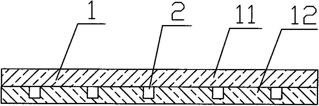
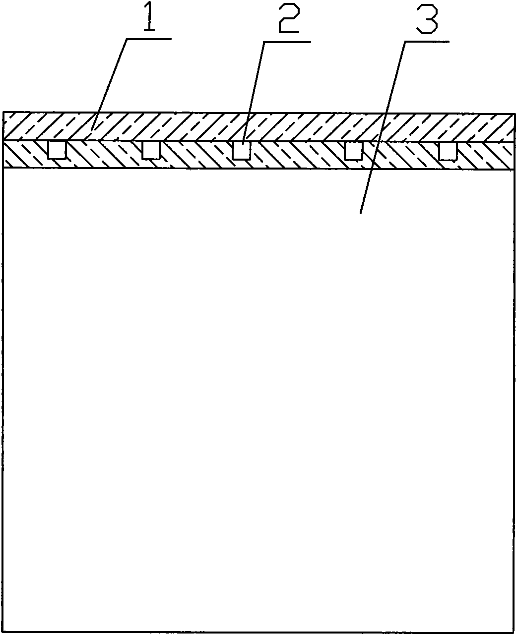
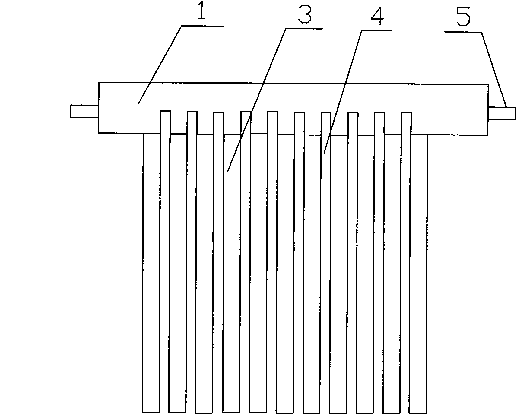
[0025] Loading plates for debonding and cleaning of silicon wafers such as figure 1 As shown, there are holes 2 distributed in the loading plate 1, the holes 2 are connected with the water pipe 5, and the cross-sectional area of ​​the holes 2 is 15-40mm 2 , the spacing between the channels 2 is 20-40mm. Preferable: the cross-sectional area of ​​channel 2 is 20mm 2 , spacing 25mm.

[0026] Further, the loading plate 1 is divided into an upper plate 11 and a lower plate 12, and there is a groove on one of the plates, and the upper plate 11 and the lower plate 12 are connected by bonding, and the grooves on the plate are closed to form a channel after bonding 2. Preferably, the groove is arranged on the lower plate 12 . After being divided into the upper plate 11 and the lower plate 12, the processing of the loading plate 1 is more convenient and t...


PUM

PropertyMeasurementUnit
Cross-sectional areaaaaaaaaaaa

Abstract

The invention relates to a method and a loading plate for degumming cleaning a crystalline silicon solar cell silicon wafer. The method mainly comprises the following steps of: bonding silicon blocks onto the loading plate distributed with porous channels, cutting the silicon blocks on a multiline cutting machine, simultaneously cutting through the porous channels of the loading plate, then connecting the porous channels with a water pipe, introducing tap water, leading the water to flow down from cut gaps, and washing away mortar bonded in the silicon wafer. By the use of the method, not only can the water consumption be greatly reduced and can water be saved by 70%, but also the cleaning effect is good, the staining rate is reduced, the quality of a product is improved, the rate of A-grade products can be improved by 1.5-2%, the cleaning time is shortened, and the labor productivity is improved by 33%; and for the loading plate for cleaning, the structure is simple, the manufacturing cost is low, the use is convenient and the production cost and the manufacturing cost of the silicon wafer are reduced.

Description

technical field [0001] The invention relates to a method for degumming and cleaning silicon wafers of crystalline silicon solar cells and tooling thereof. Background technique [0002] The existing degumming and cleaning process for silicon wafers of crystalline silicon solar cells is to put the cut silicon rods into the automatic spray tank of the pre-cleaning machine, and directly wash both sides of the silicon rods through the water jets sprayed from the nozzles on both sides of the spray tank , or spray manually through a water gun, and transfer to the next process after the spraying is completed. The current degumming cleaning process has the following problems: 1. The sprayed water enters from both sides of the silicon wafer, and it is difficult to wash away the mortar between the two adjacent silicon wafers, so that the adjacent silicon wafers cannot be separated naturally , resulting in poor cleaning effect, causing great cleaning pressure to the subsequent process,...

Claims


Application Information

Patent Timeline
IPC IPC(8): H01L21/02H01L21/00B28D5/00B08B3/02
Inventor 符云波冯时潘懋勋盛雯婷宋如来吕铁铮张凤鸣
Owner TIANWEI NEW ENERGY HLDG
Why Eureka
Try Eureka