Copper interconnection structure and forming method thereof

A copper interconnection structure, non-conformal technology, applied in the direction of electrical components, semiconductor/solid-state device manufacturing, circuits, etc., can solve the problems of metal ion 14 diffusion and affect the reliability of copper interconnection structure, so as to improve reliability, The effect of avoiding TDDB problems

Active Publication Date: 2012-06-06
SEMICONDUCTOR MANUFACTURING INTERNATIONAL (BEIJING) CORP
View PDF5 Cites 6 Cited by
  • Summary
  • Abstract
  • Description
  • Claims
  • Application Information

AI Technical Summary

Problems solved by technology

Because low-k materials and ultra-low-k materials are relatively loose and have a large number of voids, it is easier to cause the diffusion of metal ions14, causing TDDB problems and affecting the reliability of copper interconnection structures

Method used


Image

  • Copper interconnection structure and forming method thereof
  • Copper interconnection structure and forming method thereof
  • Copper interconnection structure and forming method thereof

Examples


Embodiment Construction

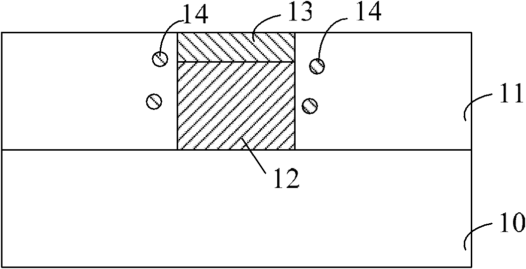
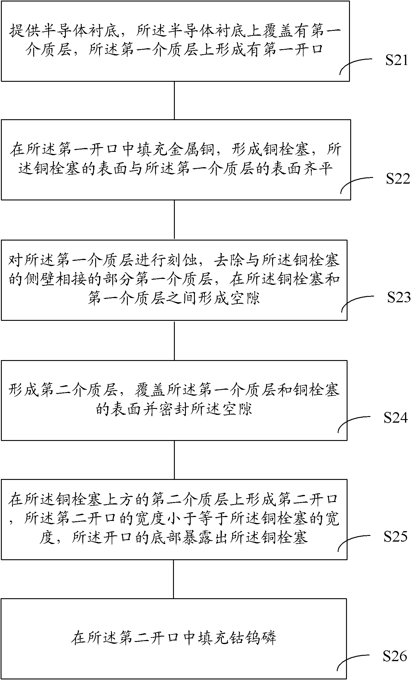
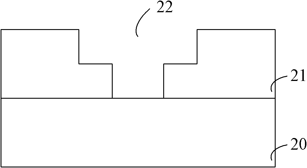
[0039] In the prior art, when cobalt-tungsten-phosphorus is formed on the surface of the copper plug, metal ions are easy to diffuse into the dielectric layer on the side wall of the copper plug, which easily leads to TDDB problems and reduces the reliability of the copper interconnection structure.

[0040] In this technical solution, a gap is formed between the copper plug and the first dielectric layer, and then a second dielectric layer is formed to cover the surfaces of the first dielectric layer and the copper plug and seal the gap, and the second dielectric layer above the copper plug A second opening is formed in the second dielectric layer and cobalt-tungsten-phosphorus is filled therein. Since there is a gap between the copper plug and the first dielectric layer, metal ions are prevented from diffusing into the first dielectric layer, and the TDDB problem is avoided, which is beneficial Improve the reliability of copper interconnect structures.

[0041] Further, afte...


PUM


Abstract

The invention provides a copper interconnection structure and a forming method thereof. The forming method of the copper interconnection structure comprises the following steps of: providing a semiconductor substrate, wherein the semiconductor substrate is covered with a first dielectric layer and a first opening is formed on the first dielectric layer; filling metal copper in the first opening to form a copper plug, wherein the surface of the copper plug is flush with the surface of the first dielectric layer; etching the first dielectric layer and removing a part of the first dielectric layer, which is connected with the side wall of the copper plug, so as to form a gap between the copper plug and the first dielectric layer; forming a second dielectric layer which covers the surfaces of the first dielectric layer and the copper plug and seals the gap; forming a second opening on the second dielectric layer above the copper plug, wherein the width of the second opening is less than the width of the copper plug and the copper plug is exposed out of the bottom of the second opening; and filling cobalt tungsten phosphorus in the second opening. Through adoption of the forming method of the copper interconnection structure, metal ions can be prevented from diffusing into the dielectric layers, thereby improving reliability.

Description

technical field [0001] The invention relates to semiconductor manufacturing technology, in particular to a copper interconnection structure and a forming method thereof. Background technique [0002] With the development of semiconductor technology, the integration level of VLSI chips has reached hundreds of millions or even billions of devices, and multi-layer metal interconnection technology with more than two layers is widely used. Traditional metal interconnects are made of aluminum metal, but with the continuous reduction of device feature size in integrated circuit chips, the current density in metal interconnect lines continues to increase, and the required response time continues to decrease. Traditional aluminum The interconnection line can no longer meet the requirements. After the process size is smaller than 130nm, the copper interconnection line technology has replaced the aluminum interconnection line technology. Compared with aluminum, metallic copper has a l...

Claims


Application Information

Patent Timeline
IPC IPC(8): H01L21/768H01L21/288
Inventor 张海洋胡敏达
Owner SEMICONDUCTOR MANUFACTURING INTERNATIONAL (BEIJING) CORP
Why Eureka
Try Eureka