Semiconductor structure and forming method thereof

A semiconductor and isolation structure technology, which is applied in the field of semiconductor structure and its formation, can solve the problems of increased production pressure and cost, poor uniformity of MOS tubes, and devices that cannot meet the requirements, so as to reduce the size of devices, avoid electric field peaks, and improve shock resistance. The effect of breakdown voltage

Pending Publication Date: 2022-03-29
SEMICON MFG INT TIANJIN +1
View PDF0 Cites 0 Cited by
  • Summary
  • Abstract
  • Description
  • Claims
  • Application Information

AI Technical Summary

Problems solved by technology

[0003] At present, there are still many problems in LDMOS devices and their manufacturing processes, which cause the devices to fail to meet the requirements
For example, electric field peaks are likely to occur at the edge of the gate at the source end, causing breakdown or TDDB problems; when forming the body region, an additional gate etching process is introduced, which increases production pressure and cost; The mask of the gate etching and ion implantation process has a large thickness and poor profile stability, and the ion implantation process has a strong dependence on the profile of the photoresist, which is likely to cause poor uniformity of the MOS tube

Method used


Image

  • Semiconductor structure and forming method thereof
  • Semiconductor structure and forming method thereof
  • Semiconductor structure and forming method thereof

Examples


Embodiment Construction

[0026] The following description provides specific application scenarios and requirements of the present application, and the objectives are to enable those skilled in the art to manufacture and use the contents of this application. Various local modifications to the disclosed embodiments will be apparent to those skilled in the art, and the general principles defined herein can be applied to other embodiments without departing from the spirit and scope of the present application. application. Therefore, the present application is not limited to the embodiment shown, but is the widest range consistent with the claims.

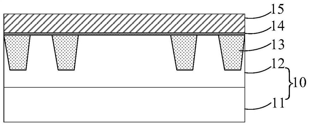
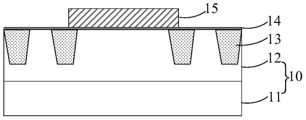
[0027] refer to figure 1 A conventional process that forms an LDMOS device includes providing a substrate 10 comprising a deep well region 11 and a drift region 12. An isolation structure 13 having a plurality of spaced distributions is formed in the drift region 12. The gate dielectric layer 14 and the gate layer 15 are sequentially deposited on the surface of the...


PUM


Abstract

The invention provides a semiconductor structure and a forming method thereof. The forming method comprises the following steps: providing a substrate, wherein the substrate comprises a drift region, and a first isolation structure and a second isolation structure which are positioned in the drift region; forming a gate structure on the surface of a part of the drift region between the first isolation structure and the second isolation structure; a first body region is formed in the drift region between the gate structure and the first isolation structure, a second body region is formed in the drift region between the gate structure and the second isolation structure, and the first body region and the second body region both extend to the lower part of the gate structure; forming a first source region and a second source region in the first body region and the second body region on the two sides of the gate structure respectively; a first drain electrode and a second drain electrode are formed in the drift region, the first drain electrode and the first source electrode are separated by a first isolation structure, and the second drain electrode and the second source electrode are separated by a second isolation structure. According to the semiconductor structure and the forming method thereof, the device performance can be optimized.

Description

Technical field [0001] The present application relates to the field of semiconductor technology, and more particularly to a semiconductor structure and a method of forming thereof. Background technique [0002] A transverse dual diffusion field effector (LDMOS, LATERAL DOUBLED MOSFET) is one of the power field effect tube, and has many advantages, for example, with better thermal stability and frequency stability, higher gain and durability. , Lower feedback capacitance and thermal resistance, and constant input impedance and simpler bias current. [0003] At present, there are still many problems with LDMOS devices and their production processes, leading to the requirements of the device. For example, the gate edge of the source is easily generated from the peak of electric field, resulting in a TDDB problem, resulting in an additional gate etching process, increasing production capacity pressure and cost when forming a body area; The mask of the gate etch and ion implantation p...

Claims


Application Information

Patent Timeline
Patent Type & Authority Applications(China)
IPC IPC(8): H01L21/336H01L29/78H01L29/06
CPCH01L29/66681H01L29/7816H01L29/0634H01L29/0653
Inventor 张全良刘丽丽
Owner SEMICON MFG INT TIANJIN
Why Eureka
Try Eureka