Raman spectrometer chip adopting arrayed waveguide grating

A technology of arrayed waveguide grating and Raman spectrometer, which is applied in the direction of optical waveguide coupling, Raman scattering, material excitation analysis, etc., can solve the problems of reduced optical performance, low wavelength resolution, large volume and weight, etc., and achieve high wavelength resolution High efficiency, high spectral resolution, small size effect

Active Publication Date: 2014-05-07
XIAMEN UNIV
View PDF11 Cites 0 Cited by
  • Summary
  • Abstract
  • Description
  • Claims
  • Application Information

AI Technical Summary

Problems solved by technology

There are many commercial products of micro-Raman spectrometers, but these products still have disadvantages such as high price, low wavelength resolution, and large volume and weight in application, such as the micro-Raman spectrometer of AhuraScientific in the United States, the palm-sized Raman spectrometer of DeltaNu in the United States, etc. Raman spectrometers, etc., have the same structure as traditional Raman spectrometers, which are the miniaturization of large spectrometers, but the reduction in optical performance is also caused by miniaturization

Method used


Image

  • Raman spectrometer chip adopting arrayed waveguide grating

Examples


Embodiment Construction

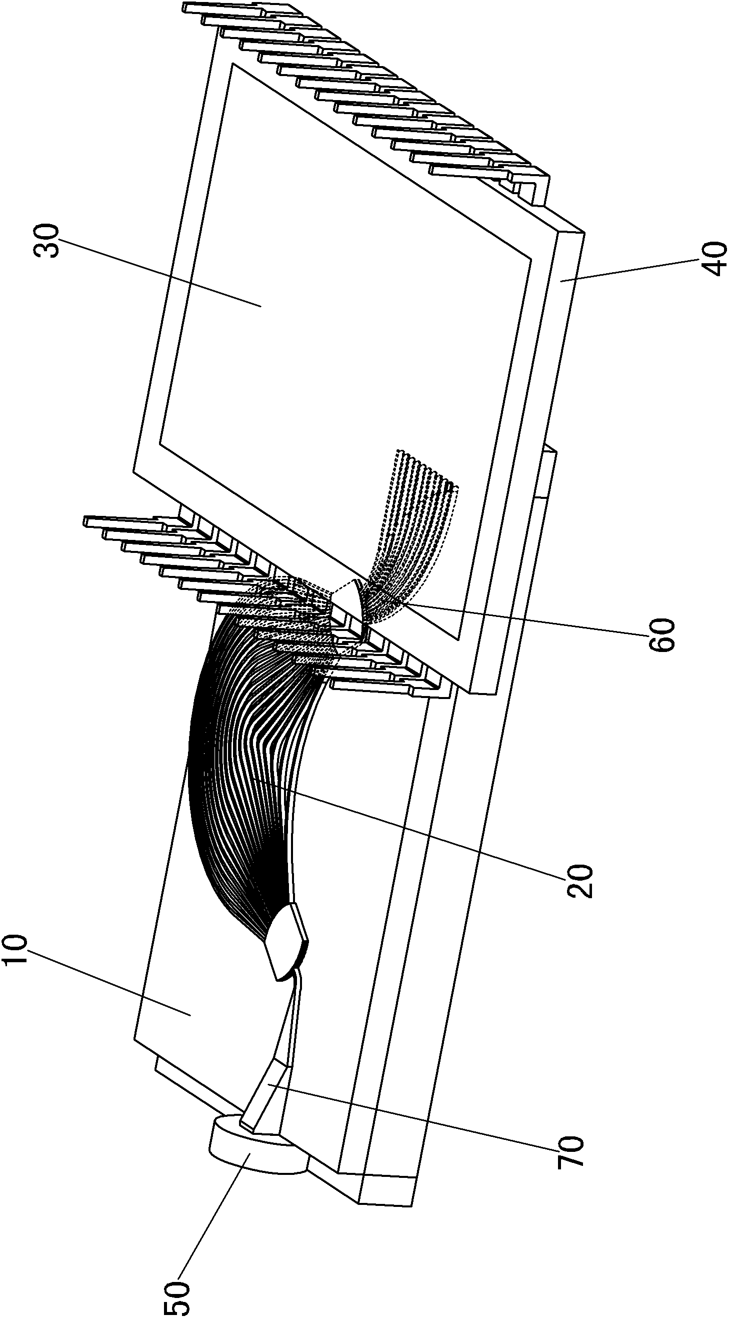
[0015] Please check figure 1 , A Raman spectrometer chip using an arrayed waveguide grating, which includes a substrate 10, an arrayed waveguide grating 20, a light conducting member 30, a photodetector array 40, an input fiber 50 and a wedge waveguide 70. The arrayed waveguide grating 20 has a waveguide array output 60 for dispersing light of different specific wavelengths into different specific waveguides, and for making different specific waveguides output light of different specific wavelengths. In this embodiment, the substrate 10 is a silicon wafer, and the light conducting member 30 is a bevel mirror.

[0016] The input fiber 50, the wedge-shaped waveguide 70, the arrayed waveguide grating 20, and the inclined mirror 30 are sequentially coupled, so that the Raman scattered light is irradiated on the photodetector through the input fiber 50, the wedge-shaped waveguide 70, the arrayed waveguide grating 20, and the inclined mirror 30 in sequence. 器Array40. In this embodimen...


PUM


Abstract

The invention discloses a Raman spectrometer chip adopting an arrayed waveguide grating, which includes a base plate, an arrayed waveguide grating, an optical conductor, a photoelectric detector array and an input optical fiber, wherein the arrayed waveguide grating, the optical conductor and the photoelectric detector array are all arranged on the base plate; the arrayed waveguide grating is provided with waveguide array output; Raman scattered light goes into the arrayed waveguide grating through the input optical fiber, so as to enable light with a specific wavelength to be output from the specific waveguide of the waveguide array output, conducted through the optical conductor, illuminated to a specific picture element of the photoelectric detector array, and converted into a digital signal; and the specific wavelength, the specific waveguide and the specific picture element are in one-to-one correspondence. The Raman spectrometer chip adopting the arrayed waveguide grating has the advantages of low price, small volume, light weight and batch production.

Description

Technical field [0001] The invention relates to a Raman spectrometer chip using an arrayed waveguide grating. Background technique [0002] Mini Raman spectrometer can measure specific chemical components, and has broad application prospects in the fields of food safety, medical and health, and environmental testing. Mini Raman spectrometers have many commercial products, but these products still have disadvantages such as high price, low wavelength resolution, large volume and weight in application, such as the mini Raman spectrometer of AhuraScientific of the United States, and the palm-type of DeltaNu of the United States. Raman spectrometers, etc., whose structure is the same as that of traditional Raman spectrometers, are the miniaturization of large-scale spectrometers, but the miniaturization also causes a decrease in optical performance. Summary of the invention [0003] The present invention provides a Raman spectrometer chip using an arrayed waveguide grating, which ove...

Claims


Application Information

Patent Timeline
Patent Type & Authority Patents(China)
IPC IPC(8): G01N21/65G02B6/34
Inventor 吕苗田中群程雅琴康怀志
Owner XIAMEN UNIV
Why Eureka
Try Eureka