

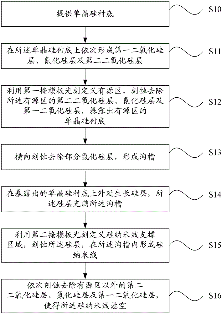
A method for preparing silicon nanowires on a single crystal silicon substrate
A technology of silicon nanowires and single crystal silicon is applied in the field of preparing silicon nanowires on a single crystal silicon substrate, which can solve the problem of high cost and achieve the effects of easy production, low cost and wide application prospect.
- Summary
- Abstract
- Description
- Claims
- Application Information
AI Technical Summary
Problems solved by technology
Method used
Image

Examples
Embodiment 1
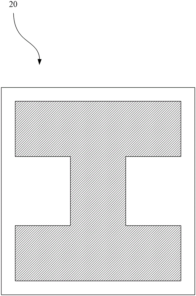
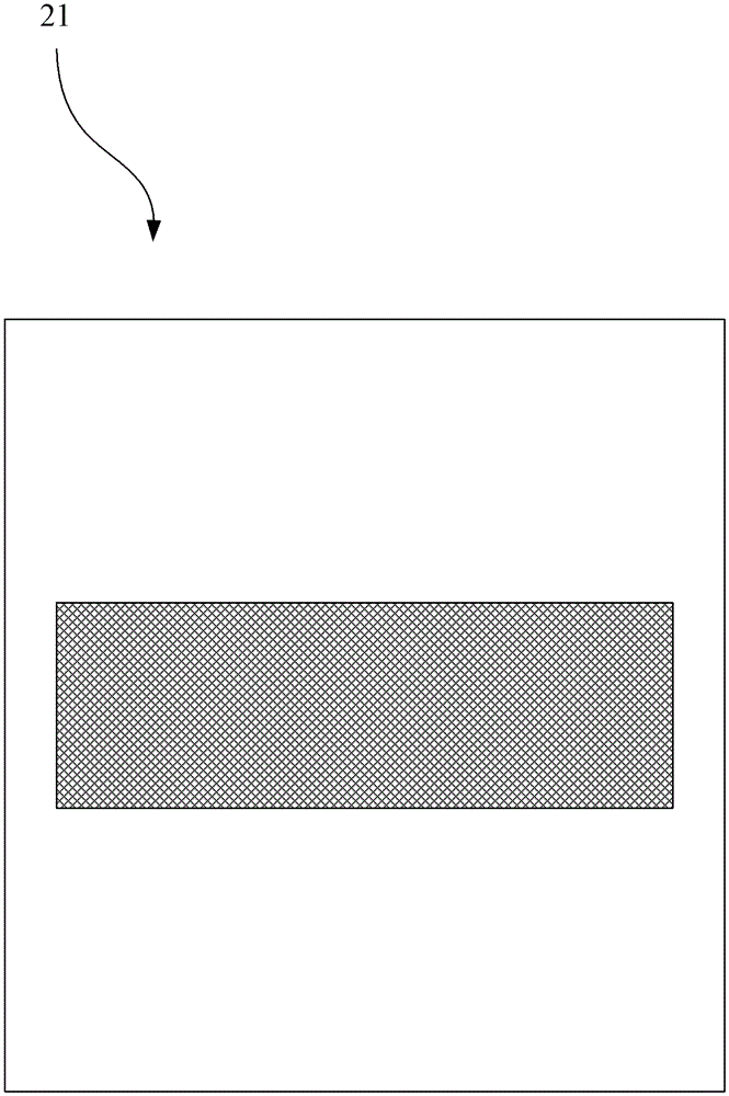
[0052] Please refer to Figure 2a-2c , Figure 3a-3g and Figure 4 ,in, Figure 2a is a schematic top view of the first mask used in the method for preparing silicon nanowires on a single crystal silicon substrate according to Embodiment 1 of the present invention; Figure 2b is a schematic top view of the second mask used in the method for preparing silicon nanowires on a single crystal silicon substrate according to Embodiment 1 of the present invention; Figure 2c It is a schematic diagram of registration with the first mask when the second mask is used in the method for preparing silicon nanowires on a single crystal silicon substrate according to Embodiment 1 of the present invention; Figure 3a-3g It is the method for preparing silicon nanowires on a single crystal silicon substrate according to Embodiment 1 of the present invention. Figure 2c Schematic diagram of the cross-sectional process in the direction indicated by AA' in the middle; Figure 4 It is the metho...
Embodiment 2
[0065] Please refer to Figures 5a-5c and Image 6 ,in, Figure 5a is a schematic top view of the first mask used in the method for preparing silicon nanowires on a single crystal silicon substrate according to Embodiment 2 of the present invention; Figure 5b is a schematic top view of the second mask used in the method for preparing silicon nanowires on a single crystal silicon substrate according to Embodiment 2 of the present invention; Figure 5c It is a schematic diagram of registration with the first mask when the second mask is used in the method for preparing silicon nanowires on a single crystal silicon substrate according to Embodiment 2 of the present invention; Image 6 It is the method for preparing silicon nanowires on a single crystal silicon substrate according to the second embodiment of the present invention. Figure 5c The schematic cross-sectional view in the direction indicated by AA'.
[0066] The difference between this embodiment and Embodiment 1 i...
PUM
| Property | Measurement | Unit |
|---|---|---|
| thickness | aaaaa | aaaaa |
| thickness | aaaaa | aaaaa |
| thickness | aaaaa | aaaaa |
Abstract
Description
Claims
Application Information