

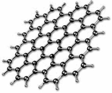
Electrically-induced reduction method for degraded graphene oxide
A graphene oxide, electric induction technology, applied in the reduction of graphene oxide, preparation and nano-etched graphene field, can solve the problem of zero band gap characteristic barrier and so on
- Summary
- Abstract
- Description
- Claims
- Application Information
AI Technical Summary
Problems solved by technology
Method used
Image

Examples
Embodiment Construction
[0018] The method of using a conductive atomic force microscope to electrically induce the reduction of graphene oxide proposed by the present invention is relatively stable and reliable, and can be used as a conventional means to complete the reduction of graphene oxide. Described below is an embodiment of using a conductive atomic force microscope to electrically induce the reduction of graphene oxide proposed by the present invention.
[0019] In the drawings, for the convenience of illustration, the size of lines and structures does not represent the actual size. Although these diagrams do not completely and accurately reflect the actual scale of the instrument and circuit, they still completely reflect the general working principle of the instrument and the basic structure of the working circuit during the reduction process.
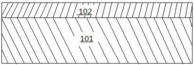
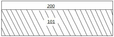
[0020] Firstly, the cleaned silicon substrate 101 is doped to form a highly doped substrate. Among them, the doping method is ion implantation, an...
PUM
 Abstract
Description
Claims
Application Information