

Trapped charge capture type flash memory array structure and operation method thereof
A memory array and trap charge technology, applied in the field of flash memory array structure, can solve the problems of complex peripheral control circuits, high power consumption of non-volatile memory, and low storage density
- Summary
- Abstract
- Description
- Claims
- Application Information
AI Technical Summary
Problems solved by technology
Method used
Image

Examples
Embodiment Construction
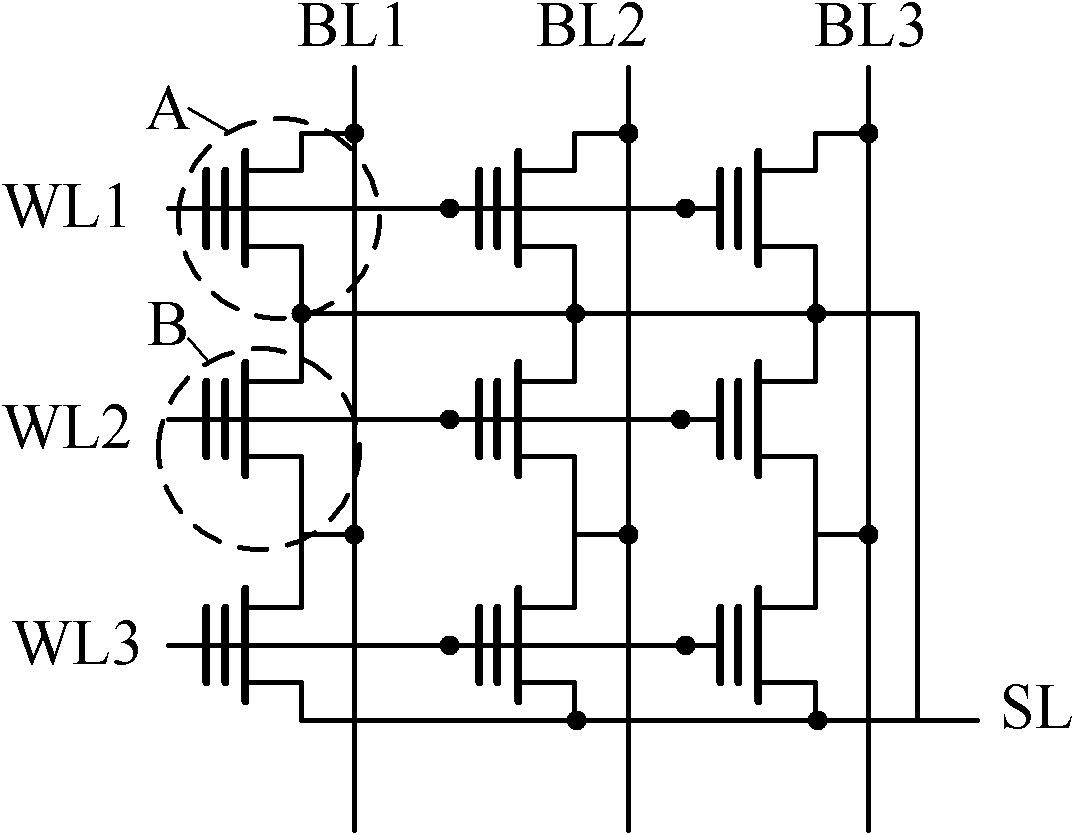
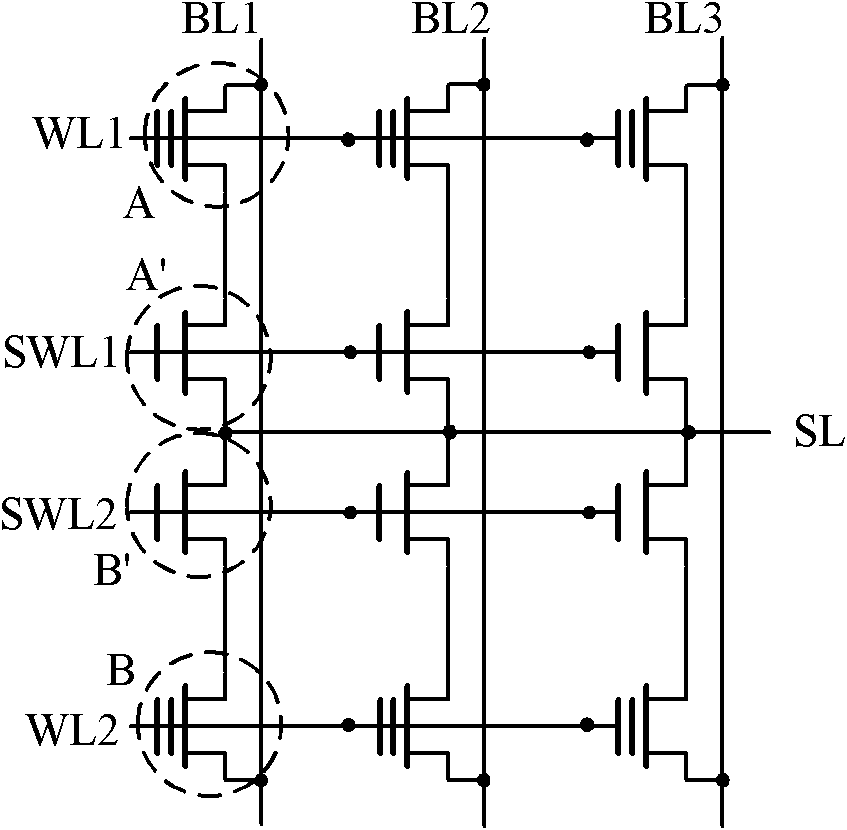
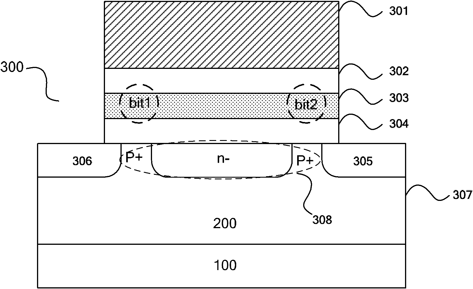
[0031]Embodiments of the present invention are described in detail below, examples of which are shown in the drawings, wherein the same or similar reference numerals designate the same or similar elements or elements having the same or similar functions throughout. The embodiments described below by referring to the figures are exemplary only for explaining the present invention and should not be construed as limiting the present invention.
[0032] In describing the present invention, it should be understood that the terms "center", "longitudinal", "transverse", "upper", "lower", "front", "rear", "left", "right", " The orientations or positional relationships indicated by "vertical", "horizontal", "top", "bottom", "inner", "outer", etc. are based on the orientation or positional relationships shown in the drawings, and are only for the convenience of describing the present invention and simplifying Describes, but does not indicate or imply that the device or element referred ...
PUM
 Abstract
Description
Claims
Application Information