Imaging optical microfluid sensing device and method thereof

A sensing device and microfluidic technology, applied in the fields of photobiology and chemical sensing, can solve problems such as the inability to achieve high-throughput rapid measurement, and achieve the effect of easy realization and mass production

Inactive Publication Date: 2013-08-14
TIANJIN UNIV
View PDF3 Cites 0 Cited by
  • Summary
  • Abstract
  • Description
  • Claims
  • Application Information

AI Technical Summary

Problems solved by technology

[0005] The purpose of the present invention is to solve the problem that the above-mentioned microresonance sensing multiplexing technology still cannot realize high-throughput rapid measurement, and to provide an imaging optical microfluidic sensing device and method

Method used


Image

  • Imaging optical microfluid sensing device and method thereof
  • Imaging optical microfluid sensing device and method thereof
  • Imaging optical microfluid sensing device and method thereof

Examples


Embodiment 1

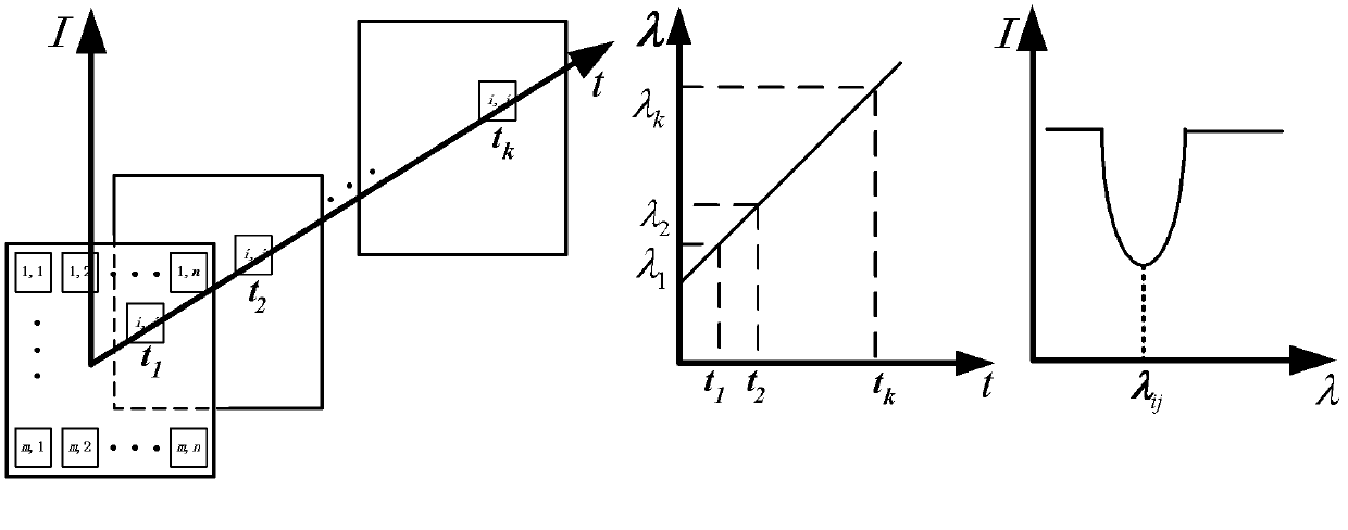
[0031] Embodiment 1: The principle of signal control and processing unit to detect the resonant wavelength of optical microfluidic resonant cavity

[0032] Each pixel unit of the m×n array photodetector is in one-to-one correspondence with each unit in the m×n optical microfluidic resonant cavity array, wherein m is the number of rows, and n is the number of columns. Such as figure 1 As shown, for the (i, j)th pixel unit of the m×n array photodetector, i=1, Λ, m, j=1, Λ, n, the signal control and processing unit continuously tunes the laser output wavelength, The output wavelength varies with time t, at t 1 , t 2 ......t k At different times, the corresponding light wavelengths are λ 1 ,λ 2 ,Λ,λ k , while tuning, synchronously control the array photodetector to record the image P corresponding to each light wavelength 1 , P 2 ,Λ,P k . The signal control and processing unit extracts the series of images, that is, extracts the (i, j)th pixel P for each image l (i, j),...

Embodiment 2

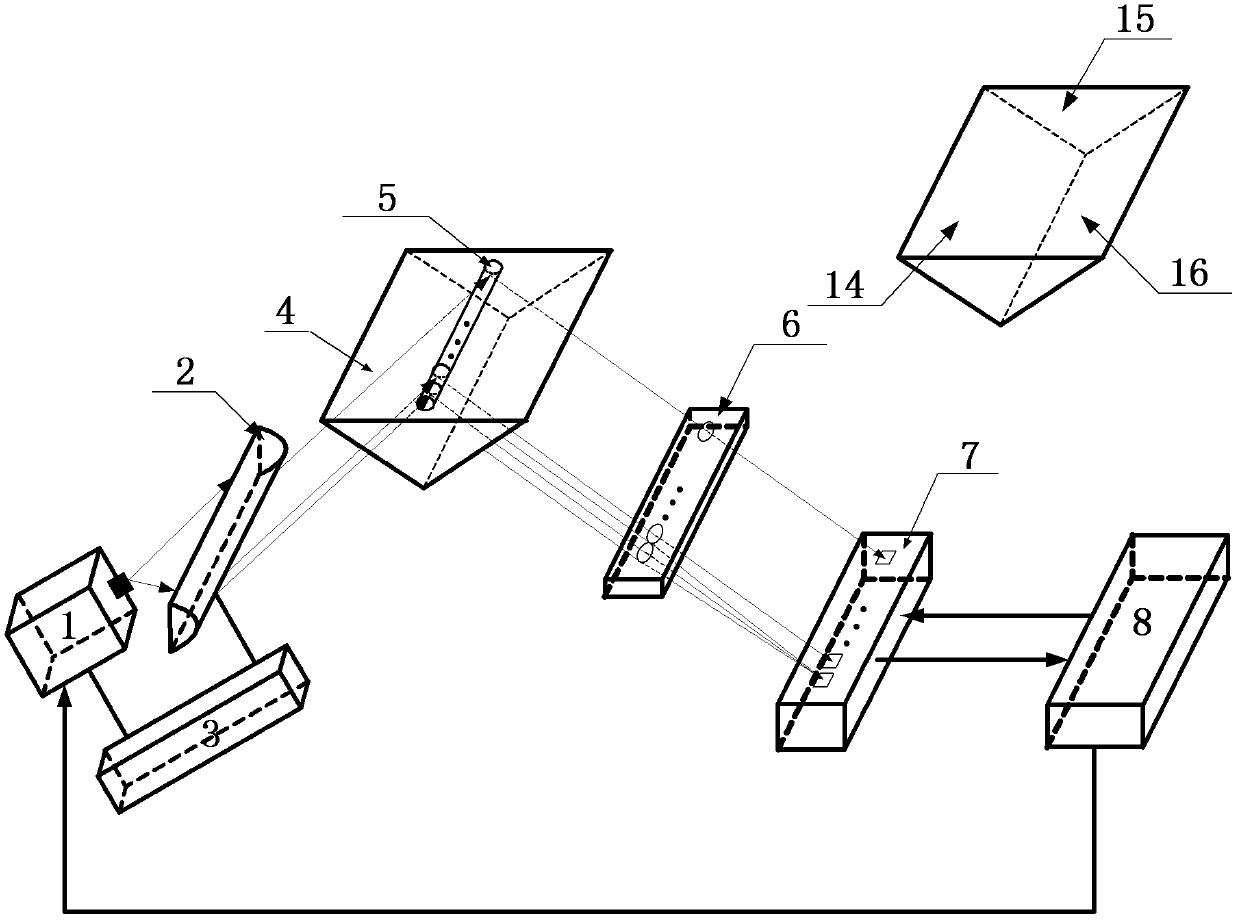
[0033] Embodiment 2: A sensing device and method using a one-dimensional optical-microfluidic resonant cavity array based on different positions of a single microtube along the axial direction

[0034] Such as figure 2 As shown, the sensing device includes: a tunable laser light source 1 is located on an incident angle adjustment frame 3 and is connected to a signal control and processing unit 8. The tunable laser light source is an erbium-doped tunable fiber laser with a wavelength range of 1525 to 1560 nm; The surface collimator lens 2 is located on the incident angle adjustment frame 3, and its plane part is perpendicular to the optical axis of the tunable laser light source 1; the reflective prism 4 is a right-angle prism, and the size of its reflective surface 15 is 24mm×36mm, and the incident angle of the reflective prism 4 The surface 14 is facing the convex surface of the collimating lens 2, and the outgoing surface 16 of the reflecting prism 4 is facing the linear mi...

Embodiment 3

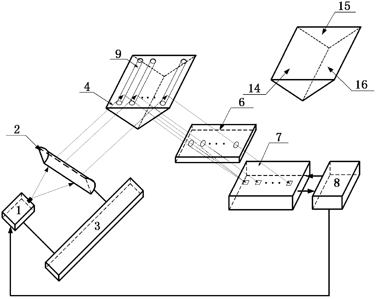
[0037] Embodiment 3: A sensing device and method using a one-dimensional optical-microfluidic resonant cavity array based on multiple microtubes arranged side by side

[0038] Such as image 3 As shown, the sensing device includes: a tunable laser light source 1 is located on an incident angle adjustment frame 3 and is connected to a signal control and processing unit 8. The tunable laser light source is an erbium-doped tunable fiber laser with a wavelength range of 1525 to 1560 nm; The surface collimator lens 2 is located on the incident angle adjustment frame 3, and its plane part is perpendicular to the optical axis of the tunable laser light source 1; the reflective prism 4 is a right-angle prism, and the size of its reflective surface 15 is 24mm×36mm, and the incident angle of the reflective prism 4 The surface 14 is facing the convex surface of the collimating lens 2, and the outgoing surface 16 of the reflective prism 4 is facing the linear microlens array 6, and the re...


PUM

PropertyMeasurementUnit
refractive indexaaaaaaaaaa

Abstract

Disclosed are an imaging optical microfluid sensing device and a method thereof. The sensing device comprises a tunable laser light source, a collimating lens, an incidence angle adjusting rack, a reflection prism, an optical microfluid resonant cavity array, a microlens array, an array photoelectric detector, and a signal control and processing unit. Lights emitted from the light source pass through the collimating lens and become parallel light beams, which are incident on the reflection prism. The incident lights at the bottom of the reflection prism are coupled through an evanescent fieldso as to excitate resonant mode of the optical microfluid resonant cavity array for sensing. The reflected lights with the wavelength information of the resonant mode are incident on the array photoelectric detector for imaging. When continuously tuning laser light output wavelength, corresponding multiple-frame images are recorded. Serial processing is carried out on each pixel in the array photoelectric detector in the signal processing unit according to record light source wavelength, so as to realize wavelength sensing querying of each optical microfluid resonant cavity. The apparatus caneffectively realize multichannel optical microfluid sensing and can be used for the construction of a high-flux optical microfluid detection system.

Description

technical field [0001] The invention relates to the field of various multi-channel multiplexing technologies based on optical micro-resonance sensing, especially the space-division multiplexing of optical microfluidic sensing, which belongs to photobiological and chemical sensing technologies. Background technique [0002] The label-free biosensor based on microresonant optical technology directly measures molecular interactions, which can realize real-time observation of biomolecular interactions. Since the analyte to be measured does not need special properties such as fluorescence, characteristic absorption or scattering bands, the range of measurement objects is greatly expanded. It can detect toxins, proteins, DNA, and even the entire cell behavior, thus providing a powerful analytical tool for medical diagnosis, drug development, food monitoring, environmental monitoring and other fields. [0003] The optical microfluidic resonator uses total reflection to completely c...

Claims


Application Information

Patent Timeline
Patent Type & Authority Patents(China)
IPC IPC(8): G01N21/43G02B7/02G02B7/18
Inventor 江俊峰刘铁根刘琨刘文辉
Owner TIANJIN UNIV
Why Eureka
Try Eureka