Technological method for planarization of radio frequency LDMOS polysilicon channel

A process method and polysilicon technology, applied in electrical components, semiconductor/solid-state device manufacturing, circuits, etc., can solve the problems of discontinuous metal silicide and increase in on-resistance, and achieve the advantages of increasing the window and reducing the on-resistance. Effect

Inactive Publication Date: 2012-06-27
SHANGHAI HUAHONG GRACE SEMICON MFG CORP
View PDF3 Cites 7 Cited by
  • Summary
  • Abstract
  • Description
  • Claims
  • Application Information

AI Technical Summary

Problems solved by technology

However, since the depth of the trench is deep and the thickness of the polysilicon filling is relatively thick, the polysilicon above the trench will form a depression. At the same time, the polysilicon deposition itself will also make the surface uneven, which will be maintained when the subsequent polysilicon is etched back. Rugged topography, which leads to discontinuity in the formed metal silicide, which in turn leads to increased on-resistance of RF LDMOS

Method used


Image

  • Technological method for planarization of radio frequency LDMOS polysilicon channel
  • Technological method for planarization of radio frequency LDMOS polysilicon channel
  • Technological method for planarization of radio frequency LDMOS polysilicon channel

Examples


Embodiment Construction

[0021] In order to have a more specific understanding of the technical content, characteristics and effects of the present invention, now in conjunction with the illustrated embodiment, the details are as follows:

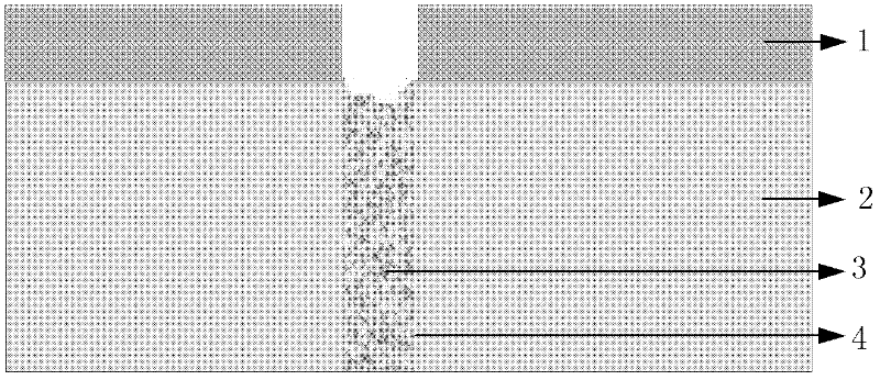
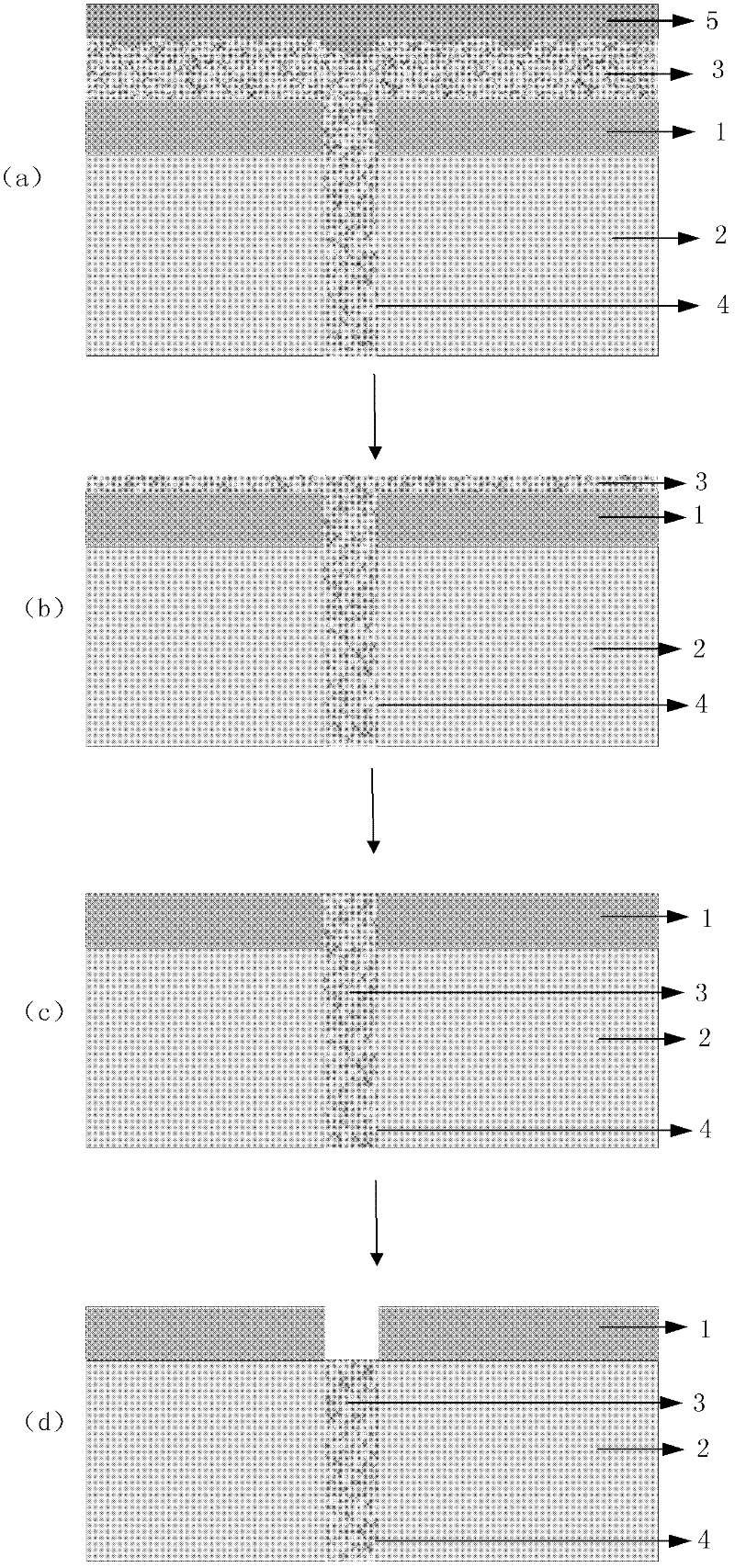
[0022] see image 3 As shown, the radio frequency LDMOS polysilicon channel planarization process method of this embodiment, after the polysilicon 3 is deposited, according to the following steps, the surface of the polysilicon 3 in the channel 4 is planarized:

[0023] In step 1, a bottom organic anti-reflection layer 5 is evenly coated on the polysilicon 3 by using the fluidity of organic matter, as shown in Figure 3 (a).

[0024] The coating thickness is greater than the sum of the drop caused by the uneven surface of the polysilicon 3 and the depression at the top of the polysilicon 3 in the channel 4 . Since the maximum drop on the surface of the polysilicon 3 can reach 1500 angstroms, the thickness of the coated bottom organic anti-reflective layer 5 should ...


PUM


Abstract

The invention discloses a technological method for planarization of a radio frequency LDMOS polysilicon channel. After polysilicon deposition is carried out, in order to carry out planarization processing on a surface of a polysilicon channel, the method is implemented by the following steps that: (1), a bottom organic antireflective layer is coated; (2), etchback is carried out on the bottom organic antireflective layer; (3), main etching is carried out on the polysilicon to remove polysilicon that is outside the channel; and (4), over etching is carried out on the polysilicon to enable the polysilicon surface inside the channel to be planarized. According to the method provided in the invention, before the etchback of the polysilicon, the bottom organic antireflective layer is coated to carry out planarization; and a dry etching technology with a low selection ratio is utilized to carry out etchback, so that roughness drop of the polysilicon surface inside the channel is reduced; therefore, continuous metal silicide can be formed; and objectives that conductive resistance of the RF LDMOS is reduced and a subsequent technological window is increased can be achieved.

Description

technical field [0001] The invention relates to the field of semiconductor integrated circuits, in particular to a process method for planarizing a radio frequency LDMOS polysilicon channel. Background technique [0002] In RF LDMOS (Radio Frequency Lateral Diffusion Metal Oxide Field Effect Transistor), in order to lead the current from the front to the back, a deep trench will be formed on the silicon substrate, and doped polysilicon will be filled in the deep trench. The front side is connected to the heavily doped region at the bottom of the deep trench, thereby directing the current from the front side to the back side. [0003] In order to connect the polysilicon surface in the channel with the contact via hole to form an ohmic contact, it is necessary to form a metal silicide on the polysilicon surface. However, since the depth of the trench is deep and the thickness of the polysilicon filling is relatively thick, the polysilicon above the trench will form a depressi...

Claims


Application Information

Patent Timeline
Patent Type & Authority Applications(China)
IPC IPC(8): H01L21/336H01L21/306
Inventor 吴智勇
Owner SHANGHAI HUAHONG GRACE SEMICON MFG CORP
Why Eureka
Try Eureka