Packaging method for high-efficiency vertical coupling interconnection of optical fiber and optical waveguide chip

A technology of vertical coupling and packaging method, applied in the field of integrated optics, which can solve the problems of demanding fiber incident angle, inability to achieve repeatable operation, and high stability requirements of the coupling system, to achieve anti-interference array integration, overcome instability and The effect of repeatable alignment, easy array integration

Inactive Publication Date: 2012-07-04
ZHONGBEI UNIV
View PDF3 Cites 35 Cited by
  • Summary
  • Abstract
  • Description
  • Claims
  • Application Information

AI Technical Summary

Problems solved by technology

However, the use of vertical grating coupling has strict requirements on the incident angle of the fiber, and the stabili

Method used


Image

  • Packaging method for high-efficiency vertical coupling interconnection of optical fiber and optical waveguide chip
  • Packaging method for high-efficiency vertical coupling interconnection of optical fiber and optical waveguide chip
  • Packaging method for high-efficiency vertical coupling interconnection of optical fiber and optical waveguide chip

Examples


Embodiment Construction

[0030] A preferred embodiment will be given below, and the present invention will be described more clearly and completely in conjunction with the accompanying drawings.

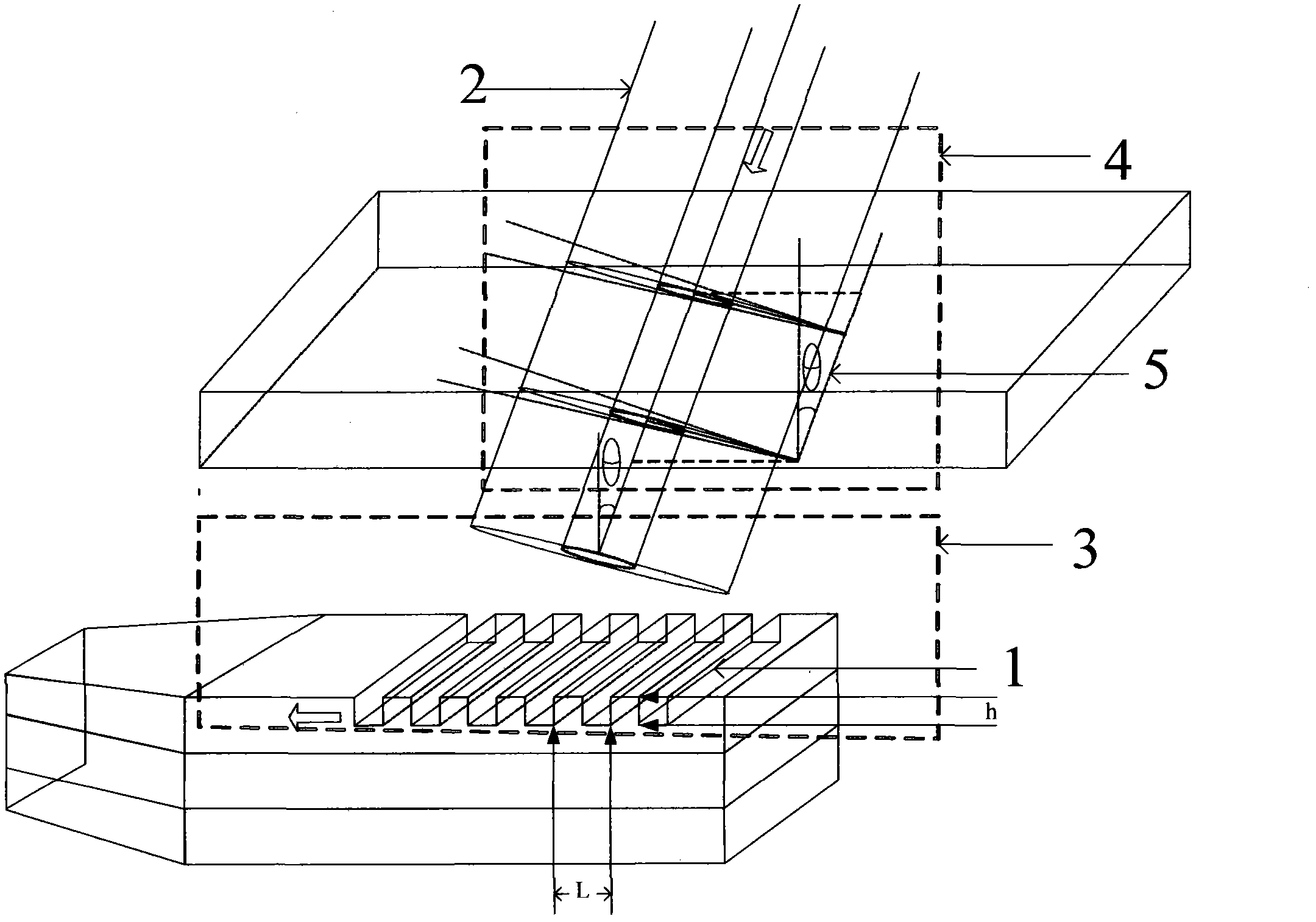
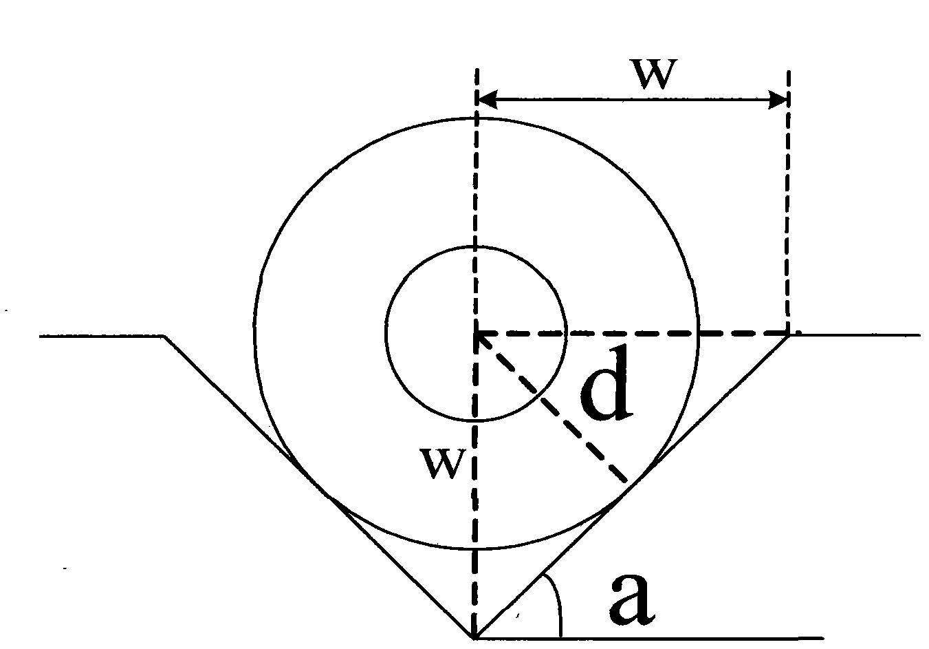
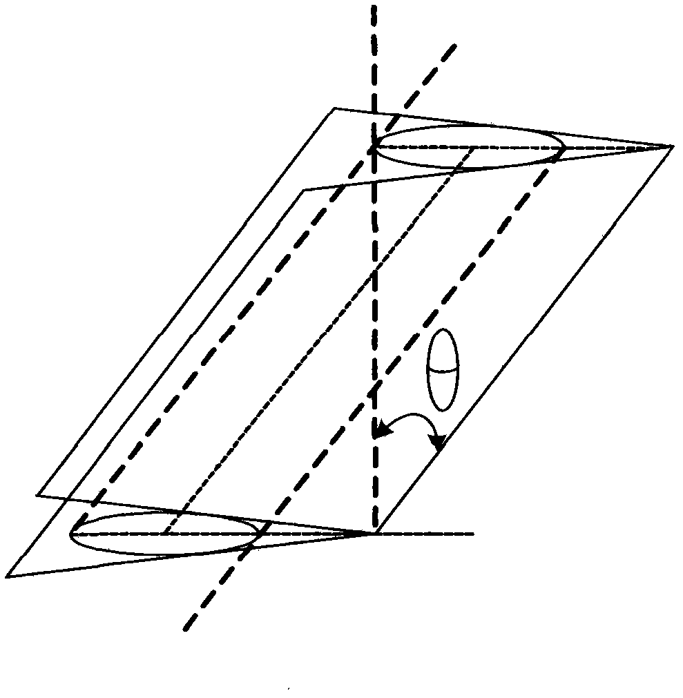
[0031] Such as figure 1 As shown, the coupling package structure includes a silicon-based nanowaveguide grating 1, a single-mode fiber 2, an inner package (coupling package end) 3, an outer package 4, and a V-shaped fiber positioning groove 5. The inclination angle of the V-shaped fiber positioning groove 5 is theta. The inner package is formed by dispensing and curing the refractive index matching paste coated on the surface of the grating and the planed vertical optical fiber by dispensing and curing the low refractive index ultraviolet curing adhesive material. The external packaging body is mainly composed of an external packaging box containing the entire grating and an internal packaging body, and its top has a through V-shaped optical fiber positioning groove. The duty ratio of the silicon-based nan...


PUM

PropertyMeasurementUnit
Mode field diameteraaaaaaaaaa

Abstract

The invention discloses a packaging method for high-efficiency vertical coupling interconnection of optical fiber and optical waveguide chip which comprises the following steps of: preparing a silica-based nano waveguide grating and scanning the silica-based nano waveguide grating by applying a scanning electron microscope; preparing a curing packaging material with a low refractive index; preparing a monomode optical fiber; coating an optical anti-reflection film on the surface of the silica-based nano waveguide grating; regulating the position between the monomode optical fiber and the silica-based nano waveguide grating; dispensing an adhesive at the coupling ends of the monomode optical fiber and the silica-based nano waveguide grating; exposing and curing an inner packaged body subjected to adhesive dispensing; preparing a V-shaped optical fiber positioning groove; placing the monomode optical fiber in the V-shaped optical fiber positioning groove; carrying out curing packaging on the monomode optical fiber; exposing and curing the V-shaped optical fiber positioning groove subjected to adhesive dispensing; and testing the finally packaged structure. The invention overcomes the defects of instability and the like of a nano waveguide and grating vertical coupling system on the existing optical integrated chip. The packaged structure provided by the invention has simple structure and high stability, resists external interference and is easy for array integration.

Description

technical field [0001] The invention belongs to the field of integrated optics, in particular to a packaging method for efficient vertical coupling and interconnection of an optical fiber and an optical waveguide chip. Background technique [0002] With the development of high-speed information technology, the development of integrated optical devices has become an inevitable trend in the interlaced development of various fields such as optical communication, optical computing, and optical sensing in the future. At the same time, it also has great potential application value in the fields of micro-optical devices, optical quantum devices, precision time-frequency measurement, optical integration, high-sensitivity sensors, optical networks, and optical quantum computers. The silicon-based integrated unit optical interconnection system is an interconnection system that uses light as the transmission signal and is composed of various silicon-based optical waveguide devices incl...

Claims


Application Information

Patent Timeline
IPC IPC(8): G02B6/34
Inventor 苏淑靖焦新泉薛晨阳臧俊斌闫树斌张文栋仝晓刚晋玉剑王景雪崔丹凤韦丽萍王永华田学东
Owner ZHONGBEI UNIV
Why Eureka
Try Eureka