Substrate processing device and method

A technology of a substrate processing device and a substrate processing method, which is applied in the directions of optics, instruments, and optomechanical equipment, and can solve problems such as reduction, poor development, resist pattern film thickness deviation, resist pattern dimensional accuracy, etc.

Inactive Publication Date: 2012-07-04
LAPIS SEMICON CO LTD
View PDF5 Cites 2 Cited by
  • Summary
  • Abstract
  • Description
  • Claims
  • Application Information

AI Technical Summary

Problems solved by technology

[0004] However, in the spray development method, there is a problem that when the same spray nozzle is used to continuously perform development on a plurality of wafers, the developer remains in the vicinity of the discharge port at the tip of the spray nozzle and becomes a droplet, which drops onto the photosensitive resin. film
The developer remaining near the discharge port at the tip of the spray nozzle is degraded by contact with the outside air. Therefore, when the remaining developer drops on the photosensitive resin film before the fresh developer, there is a risk of poor development.
In this case, there is a problem that the film thickness of the resist pattern varies or the dimensional accuracy of the resist pattern (for example, the dimensional accuracy of the minute openings) decreases.

Method used


Image

  • Substrate processing device and method
  • Substrate processing device and method
  • Substrate processing device and method

Examples


Embodiment approach 1

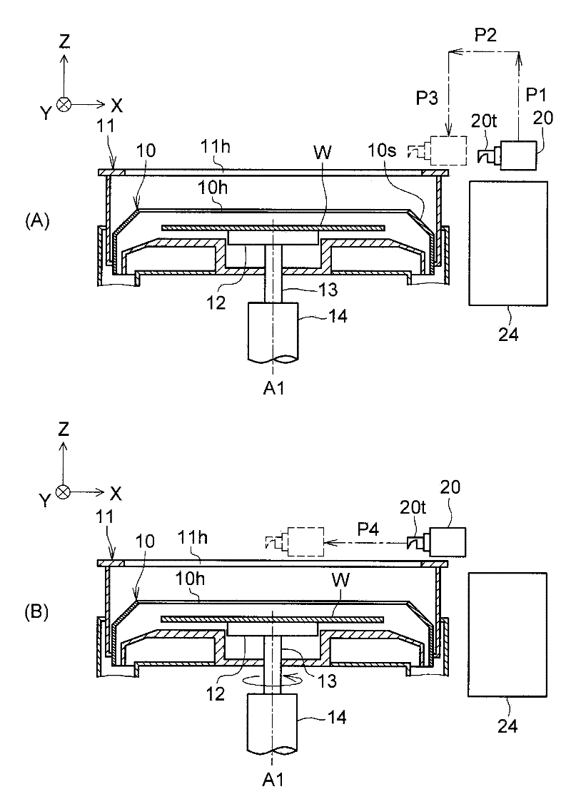
[0050] figure 1 is a diagram schematically showing the main configuration of a developing device 1 as a substrate processing device according to Embodiment 1 of the present invention, figure 2 is showing figure 1 A plan view of a part of the developing device 1 is shown. shown in schematic section figure 1 part of the structure. Such as figure 1 As shown, the developing device 1 has: a rotary disk (support member) 12 supporting the back surface of a semiconductor wafer W (hereinafter, simply referred to as “wafer W”); The developing device 1 is a device for performing development treatment by a spray development method on a photosensitive resin film (not shown) which is a film to be processed formed on the upper surface of the wafer W. As shown in FIG. The photosensitive resin film is a resist film formed by applying, for example, a spin coating method. Before the wafer W is loaded into the developing device 1, it is exposed with light passing through the mask blank by ...

Embodiment approach 2

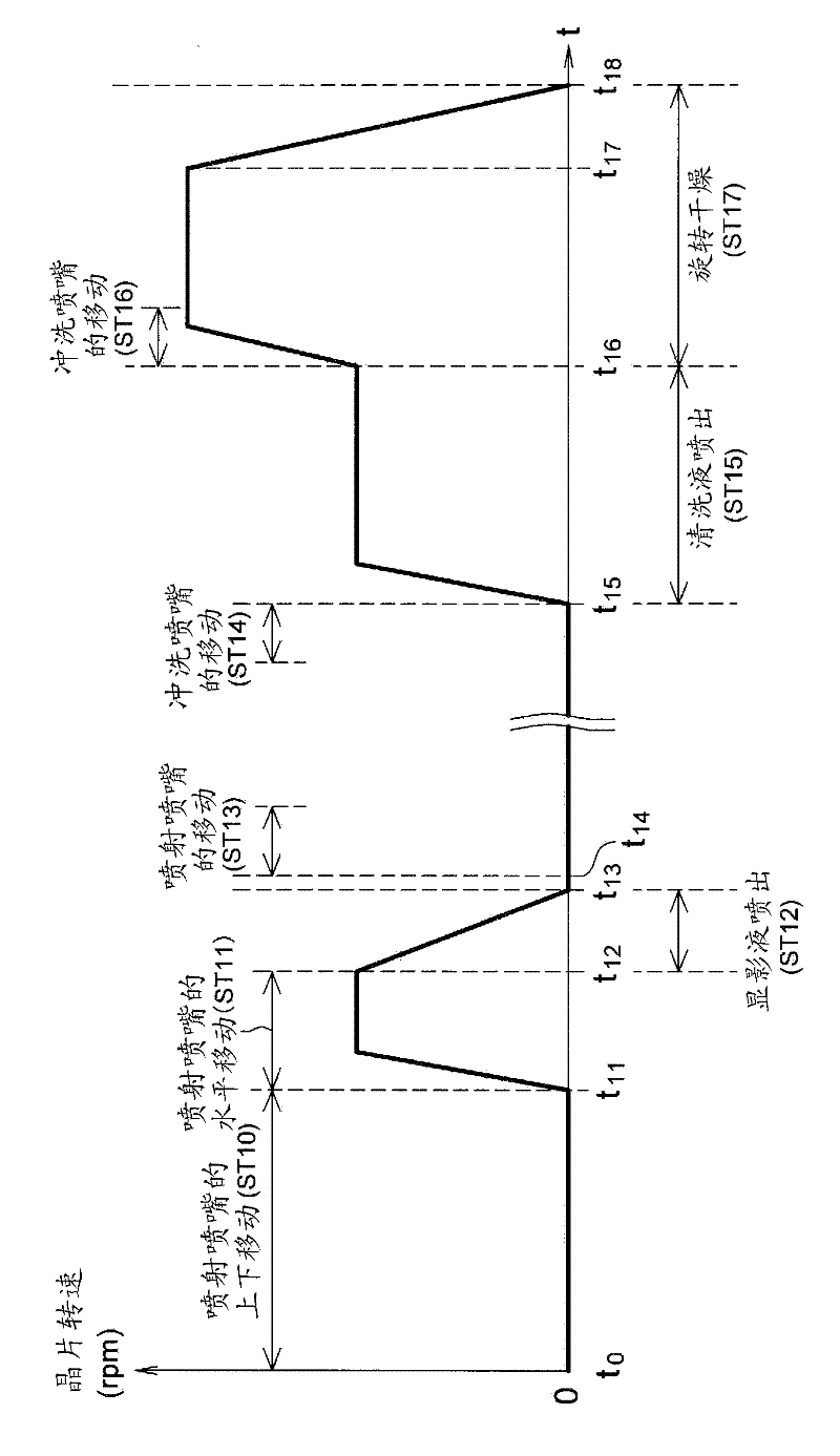
[0072] Next, Embodiment 2 of the present invention will be described. The developing device of Embodiment 2 has the same configuration as that of the developing device of Embodiment 1 except for the order of the developing process. Figure 8 It is a timing chart schematically showing an example of the sequence of the development process in the second embodiment.

[0073] As in the case of Embodiment 1, when the sequence starts, the spray nozzle moving mechanism 21 moves the spray nozzle 20 up and down (step ST10 ). Specifically, as Figure 4 As shown in (A), the ejection nozzle moving mechanism 21 raises the ejection nozzle 20 on the path P1, moves it horizontally on the path P2, and lowers the ejection nozzle 20 to a position outside the outer edge of the wafer W on the path P3.

[0074] Then, the ejection nozzle moving mechanism 21 moves the ejection nozzle 20 in the horizontal direction so that the tip portion 20t of the ejection nozzle 20 is located at the ejection posit...

Embodiment approach 3

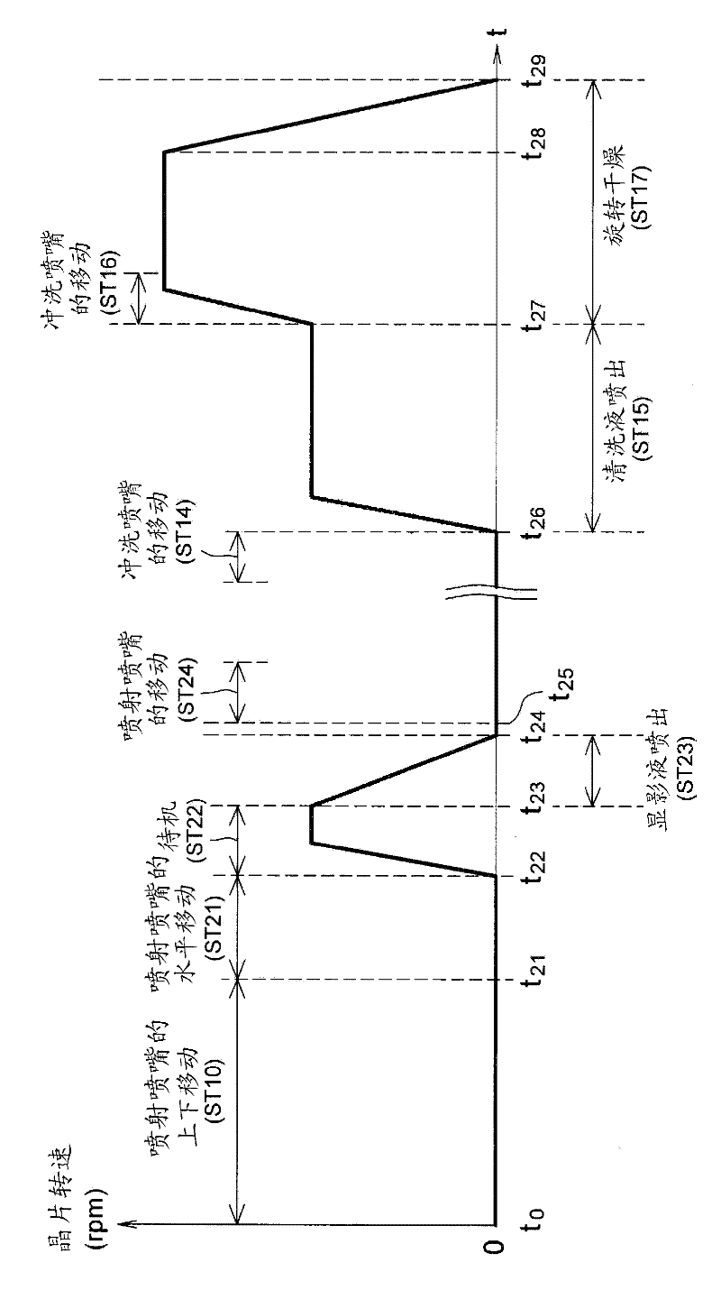
[0079] Next, Embodiment 3 of the present invention will be described. The developing device of Embodiment 3 has the same configuration as that of the developing device 1 of Embodiment 1 except for the order of the developing process. Figure 9 It is a timing chart schematically showing an example of the sequence of the developing process in the third embodiment.

[0080] Such as Figure 9 As shown in , the developer discharge control unit 44 reaches the discharge position at a predetermined time t after the spray nozzle 20 reaches the discharge position. 33 Time t advanced by offset time (offset time) δ (for example, 0.5 seconds) 32 The developer is started to be ejected from the ejection nozzle 20 (step ST12B). Other aspects are the same as those of Embodiment 1 image 3 in roughly the same order.

[0081] In this way, according to Embodiment 3, for example, even when the residual developer adhering to the jet nozzle 20 is scattered on the wafer W due to the impact or in...


PUM


Abstract

A semiconductor processing device sprays a liquid chemical agent onto a film on a spinning semiconductor substrate. The spray nozzle is moved horizontally from a first upper position comparatively distant from the substrate to a second upper position closer to the substrate, then vertically downward to a lower position. All of these positions are higher than the substrate and none of them overlie the substrate. The spray nozzle is then moved horizontally to a spray position over the substrate and spraying begins. Any residual liquid chemical agent remaining at the outlet of the spray nozzle from the processing of a previous substrate drops off harmlessly at the end of the downward vertical motion instead of dropping onto the film on the substrate.

Description

technical field [0001] The present invention relates to a technique of treating a film to be treated on a base material with a chemical solution. Background technique [0002] In a semiconductor manufacturing process, a resist pattern is formed on a wafer by a photolithography process, and the resist pattern is used as an etching mask. Generally, the photolithography process includes: the process of applying a photosensitive resin material (photoresist) on the processed surface of the pretreated wafer and drying it to form a photosensitive resin film; The photosensitive resin film is exposed to the light of the master plate, and the pattern of the master plate is transferred to the photosensitive resin film; in the development process, the pattern transferred to the photosensitive resin film is developed using a chemical solution (developing solution). As a developing method, for example, a spray developing method or a dip developing method is known. The jet image developm...

Claims


Application Information

Patent Timeline
Patent Type & Authority Applications(China)
IPC IPC(8): H01L21/027G03F7/30
CPCH01L21/67051G03F7/3021H01L21/6708
Inventor 德丸胜山内俊和
Owner LAPIS SEMICON CO LTD
Why Eureka
Try Eureka