Method for decreasing warp and bow of silicon carbide wafer

A bending and warping technology, applied in chemical instruments and methods, crystal growth, single crystal growth, etc., can solve problems such as epitaxial growth inconvenience, wafer cracking, etc.

Inactive Publication Date: 2012-07-04
BEIJING TIANKE HEDA SEMICON CO LTD +1
View PDF3 Cites 24 Cited by
  • Summary
  • Abstract
  • Description
  • Claims
  • Application Information

AI Technical Summary

Problems solved by technology

This high degree of warpage and curvature brings great inconvenience to the entire subsequent epitaxial growth; even during the device manufacturing process, the wafer will generate a lot of stress when it is sucked on the vacuum chuck, causing the wafer to break

Method used


Image

  • Method for decreasing warp and bow of silicon carbide wafer
  • Method for decreasing warp and bow of silicon carbide wafer

Examples


Embodiment 1

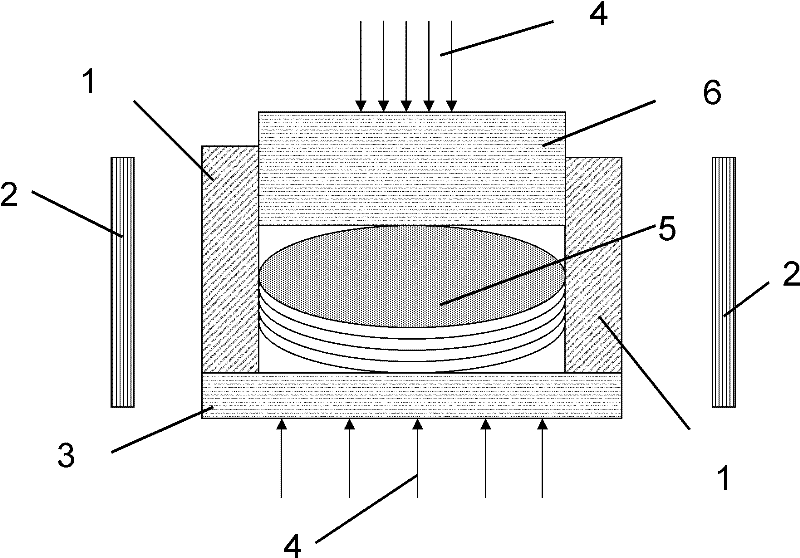
[0024] Such as figure 1 As shown, take 5 pieces of 3inch wafers that have been ground and polished, and put them between the upper platen 6 and the lower platen 6; Among them, it is required that the surfaces of the upper platen 6 and the lower platen 3 in contact with the wafer are very flat, and the warpage and curvature are all controlled to be less than 1um. Chips are stacked on top of each other and placed in figure 1 5 positions marked. Then, a pressure 4 of about 50Kg is applied on the upper and lower platens, so that the wafer is deformed flatly according to the surface shape of the platens. At the same time, the system is heated by the heater 2, and the temperature at the wafer is controlled at 1500° C. (measured by a thermocouple). After holding for 10 hours, the temperature of the wafer was gradually lowered to room temperature over 5 hours. The warpage and curvature of the wafer are measured by flatness testing equipment. The curvature Bow of the 5 wafers befor...

Embodiment 2

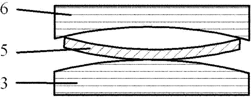
[0026] Take a 3inch wafer that has been ground and polished, such as figure 2 As shown, it is loaded between the upper platen 6 and the lower platen 6; Among them, it is required that the surfaces of the upper platen 6 and the lower platen 3 in contact with the wafer have a surface opposite to the warping of the wafer, and the warpage and curvature are all controlled at about 5um. chip placed in figure 2 5 positions marked. Then, a pressure of about 10Kg is applied on the upper and lower platens, so that the wafer is deformed in opposite directions according to the surface shape of the platens. At the same time, by heating the system, the temperature at the wafer is controlled at 1000°C (the temperature is measured with a thermocouple). After holding for 2 hours, the temperature of the wafer was gradually lowered to room temperature over 1 hour. The warpage and curvature of the wafer are measured by flatness testing equipment. The curvature Bow of the wafer before treatm...


PUM

PropertyMeasurementUnit
Mohs hardnessaaaaaaaaaa
warpageaaaaaaaaaa
warpageaaaaaaaaaa

Abstract

The invention discloses a method for decreasing warp and bow of a silicon carbide wafer, which includes the steps: applying mechanical stress on the grinded and polished silicon carbide wafer so that the wafer deforms towards the direction of flatness reduction, wherein the mechanical stress enables the wafer to reach the low warp and low bow as expected; and simultaneously, heating the wafer to the high enough temperature prior to annealing for sufficient time to enable crystal lattices of the wafer to slip and to be rearranged, so that deformation of the wafer is kept, and the wafer with the sufficiently-low warp and bow is obtained.

Description

technical field [0001] The invention relates to a method for reducing warpage and curvature of a silicon carbide wafer, in particular to a method for further reducing warpage and curvature of a silicon carbide wafer after wafer grinding and polishing. This method achieves the desired small warpage and curvature by applying a sufficiently large mechanical stress on the wafer; at the same time, high-temperature annealing treatment is performed to keep the deformation of the wafer, thereby reducing the warpage and curvature of the silicon carbide wafer. . Background technique [0002] Silicon carbide (SiC) materials have huge applications in high temperature, high frequency, high power, optoelectronics and radiation resistance due to their wide band gap, high critical breakdown electric field, high thermal conductivity, and high carrier saturation drift velocity. prospect. Compared with Si and GaAs traditional semiconductor materials, SiC has excellent properties such as high...

Claims


Application Information

Patent Timeline
Patent Type & Authority Applications(China)
IPC IPC(8): H01L21/324C30B33/02C30B29/36
Inventor 王波陈小龙刘春俊郑红军
Owner BEIJING TIANKE HEDA SEMICON CO LTD
Why Eureka
Try Eureka