Optimizing process of wafer-level packaging

A wafer-level packaging and process technology, which is applied in the manufacturing of electrical components, electrical solid-state devices, semiconductor/solid-state devices, etc., can solve problems affecting product reliability, and achieve the effects of easy control, low cost, and short process.

Inactive Publication Date: 2012-07-04
NANTONG FUJITSU MICROELECTRONICS
View PDF2 Cites 12 Cited by
  • Summary
  • Abstract
  • Description
  • Claims
  • Application Information

AI Technical Summary

Problems solved by technology

[0013] In addition, intermetallic compounds are easily penetrated between solder bumps and UBM,

Method used


Image

  • Optimizing process of wafer-level packaging
  • Optimizing process of wafer-level packaging
  • Optimizing process of wafer-level packaging

Examples


Embodiment Construction

[0031] The specific embodiments of the present invention will be described in detail below in conjunction with the accompanying drawings.

[0032] figure 2 It is a flow chart of a specific embodiment of the wafer-level packaging optimization process of the present invention, including steps:

[0033] S101, forming a bonding metal bump on the pad of the chip, the bonding metal bump being higher than the surface of the passivation layer;

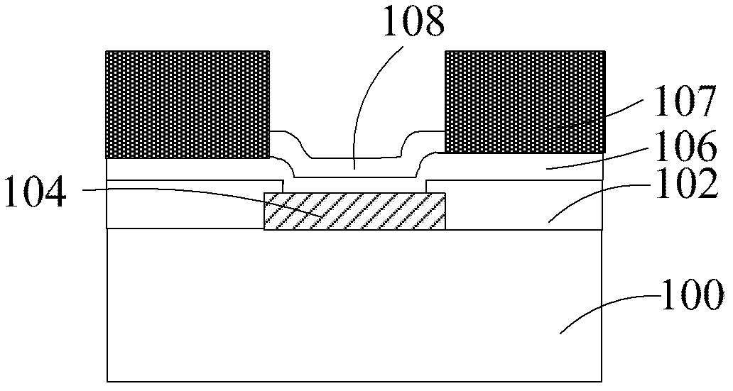
[0034] S102, forming a protective glue on the chip, the protective glue covering the passivation layer and the bonding metal bump;

[0035] S103, grinding the protective adhesive layer to expose the surface of the bonding metal bump;

[0036] S104, forming solder bumps on the surface of the exposed bonding metal bumps and reflowing them;

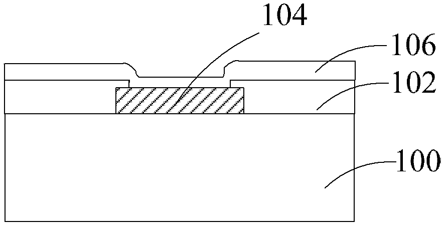
[0037] First, step S101 is performed to form a bonding metal bump on the pad of the chip, and the bonding metal bump is higher than the surface of the passivation layer, forming such as Figure 3A struc...


PUM


Abstract

The invention relates to an optimizing process of wafer-level packaging. The optimizing process comprises the following steps of: forming a bonded metal convex block on a bonding pad of a chip, wherein the bonded metal convex block is higher than the surface of a passivation layer; forming a protective adhesive on the chip, wherein the protective adhesive is used for covering the passivation layer and the bonded metal convex block; grinding a protective adhesive layer for exposing the surface of the bonded metal convex block; and forming a solder bump on the exposed surface of the bonded metal convex block and refluxing. The process disclosed by the invention has the advantages of short flow process, easiness in management and control, low cost and high performances.

Description

technical field [0001] The invention relates to the field of semiconductor device packaging, in particular to a method for forming a wafer level chip scale package (Wafer Level chip Scale Package, WLCSP). Background technique [0002] In recent years, since the microcircuit manufacturing of chips is developing toward high integration, the chip packaging also needs to develop in the direction of high power, high density, thinness and miniaturization. Chip packaging means that after the chip is manufactured, the chip is wrapped in plastic or ceramic materials to protect the chip from external moisture and mechanical damage. The main functions of the chip package are power distribution, signal distribution, heat dissipation and protection support. [0003] Since today's electronic products are required to be light, thin, small and highly integrated, the fabrication of integrated circuits will be miniaturized, resulting in an increase in the number of logic circuits contained i...

Claims


Application Information

Patent Timeline
IPC IPC(8): H01L21/60H01L21/56
CPCH01L24/11H01L2224/11H01L2924/14H01L2924/00H01L2924/00012
Inventor 石磊吴晓纯陶玉娟高国华
Owner NANTONG FUJITSU MICROELECTRONICS
Why Eureka
Try Eureka