Dummy metal filling method and integrated circuit layout structure

A redundant metal and integrated circuit technology, applied in circuits, electrical components, electric solid devices, etc., can solve problems such as large capacitance increments, and achieve the effects of small computing burden, increased computing burden, and reduced filling quantity

Active Publication Date: 2012-07-04
INST OF MICROELECTRONICS CHINESE ACAD OF SCI
View PDF1 Cites 14 Cited by
  • Summary
  • Abstract
  • Description
  • Claims
  • Application Information

AI Technical Summary

Problems solved by technology

[0005] In order to solve the problem of excessive increase in capacitance between interconnection lines after the integrated circuit is filled with redundant metal, the present invention proposes a method for filling redundant metal with different areas in different areas

Method used


Image

  • Dummy metal filling method and integrated circuit layout structure
  • Dummy metal filling method and integrated circuit layout structure
  • Dummy metal filling method and integrated circuit layout structure

Examples


Embodiment Construction

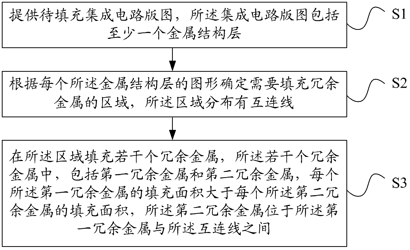
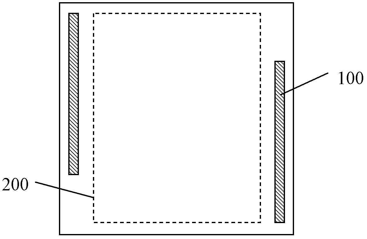
[0022] The following will clearly and completely describe the technical solutions in the embodiments of the present invention with reference to the drawings in the embodiments of the present invention. Apparently, the described embodiments are only some of the embodiments of the present invention, but not all of them. Based on the embodiments of the present invention, all other embodiments obtained by persons of ordinary skill in the art without making creative efforts belong to the protection scope of the present invention.

[0023] Secondly, the present invention is described in detail in conjunction with the schematic diagrams. When describing the embodiments of the present invention in detail, for the sake of illustration, the schematic diagrams of the interconnection lines and filling metals in the schematic diagrams will not be partially enlarged according to the general scale, and the schematic diagrams are only examples , which shall not limit the protection scope of t...


PUM


Abstract

The invention provides a dummy metal filling method. According to the invention, a plurality of dummy metals are filled in an area required to be filled by the dummy metals including first dummy metals and second dummy metals; the filling area of each first dummy metal is larger than that of each second dummy metal; and the second dummy metals are positioned between interconnection lines of the first dummy metals and the area where the dummy metals are positioned. Accordingly, the invention further provides an integrated circuit layout structure. Through the dummy metal filling method provided by the invention, the thickness consistency of an integrated circuit layout is realized, and the capacitance increment between the interconnection lines of an integrated circuit is reduced at the same time, the function of the chip is prevented from being damaged due to the introduction of the dummy metals, the dummy metals in different areas can be filled in the area required to be filled by the dummy metals, the filling number of the dummy metals is reduced, and other calculation data quality is reduced.

Description

technical field [0001] The invention relates to the fields of integrated circuit manufacturing and electronic design automation, in particular to a method for filling redundant metal on an integrated circuit layout and an integrated circuit layout structure. Background technique [0002] In the integrated circuit (Integrated Circuit, IC) manufacturing process, metals, dielectrics and other materials are fabricated on the surface of silicon wafers by various methods such as physical vapor deposition and chemical vapor deposition, forming electronic components and components. The metal structure layer of the metal interconnection line, each layer of the metal structure layer is connected with a plurality of metal-filled through holes, so that the integrated circuit has high complexity and circuit density. In the manufacture of each metal structure layer, in order to ensure the flatness of the surface of the metal structure layer, a chemical mechanical polishing (CMP) process i...

Claims


Application Information

Patent Timeline
Patent Type & Authority Applications(China)
IPC IPC(8): H01L21/768H01L27/02
Inventor 马天宇陈岚方晶晶
Owner INST OF MICROELECTRONICS CHINESE ACAD OF SCI
Why Eureka
Try Eureka