Method for improving resistance accuracy of buried resistor in PCB (printed circuit board)

A technology of PCB board and embedded resistors, which is applied in the direction of assembling printed circuits with electrical components, containing printed electrical components, etc., can solve the problems of poor resistance value accuracy and difficulty in meeting special application requirements for resistance value accuracy, so as to reduce difficulty and improve The effect of commercialization prospects

Inactive Publication Date: 2012-07-04
DONGGUAN SHENGYI ELECTRONICS
View PDF4 Cites 11 Cited by
  • Summary
  • Abstract
  • Description
  • Claims
  • Application Information

AI Technical Summary

Problems solved by technology

However, due to the limitation of silk screen printing process and equipment, the resistance value accuracy of the existing screen printing production is poor, and it is difficult to meet the special application requirements that require high resistance value accuracy.

Method used


Image

  • Method for improving resistance accuracy of buried resistor in PCB (printed circuit board)
  • Method for improving resistance accuracy of buried resistor in PCB (printed circuit board)
  • Method for improving resistance accuracy of buried resistor in PCB (printed circuit board)

Examples


Embodiment Construction

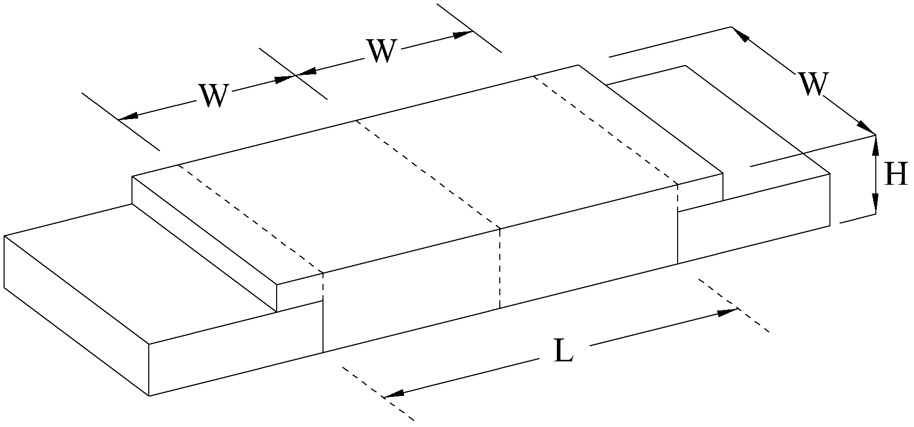
[0022] Such as figure 1 Shown is a schematic diagram of the calculation of the resistance value of the silk-printed buried resistor.

[0023] The calculation formula of buried resistance is: R=ρ×L / (W×H).

[0024] For a square resistance with a specified thickness, the formula for calculating the buried resistance is: R=R◇×L / W. In the formula, R represents the resistance value, R◇ represents the square resistance value, L represents the length of the resistance, and W represents the width of the resistance.

[0025] Square resistance value: When the resistance material is the same and the resistance thickness is the same, the resistance value of the square area per unit area is the same.

[0026] It can be seen from the definition that the square resistance value is not only related to the material properties, but also related to the resistance thickness (for example: R◇=1000Ω / square / 14μm, which means that the square resistance thickness after complete baking is required to be...


PUM


Abstract

The invention relates to a method for improving the resistance accuracy of a buried resistor in a PCB (printed circuit board), which comprises the following steps of: a step 1 of carrying out precompensation on an expected resistance of the buried resistor when the PCB is made into a finished product according to the resistance change rate of the buried resistor in the subsequent processing link so as to obtain a target resistance for making the buried resistor, and determining the length and the width of the buried resistor according to the target resistance; a step 2 of carrying out copper foil removal processing on a line layer on which the buried resistor needs to be made and making a square groove which has corresponding size and is used for accommodating the buried resistor at a preset position of the line layer; a step 3 of carrying out silk-screen printing in the square groove by adopting a screen printing plate to form a layer of resistor ink and baking and curing the resistance ink to form a buried resistor to be modified; and a step 4 of carrying out on-line dynamic modification and regulation on the buried resistor to be modified by adopting a resistor testing instrument and a laser ablation machine until the buried resistor with the target resistance is obtained. The method for improving the resistance accuracy of the buried resistor in the PCB, which is provided by the invention, can be used for obtaining the buried resistor with the high accuracy resistance.

Description

technical field [0001] The invention relates to the field of circuit board production, in particular to a method for improving the resistance value precision of embedded resistors in PCB boards. Background technique [0002] Buried resistors have the following advantages in the design of high-speed transmission circuits: improve the impedance matching of the line; shorten the signal transmission path and reduce parasitic inductance; eliminate the inductive reactance generated in the surface mount or plug-in process; reduce signal crosstalk, noise and electromagnetic interference. [0003] The embedded resistors of the existing PCB boards are usually processed with flat interlayer resistive materials (Ohmega-ply). Due to the high price of the resistive materials, the cost of the finished product is high, and the square resistance is limited (currently only 10Ω / ◇, 25Ω / ◇, 50Ω / ◇, 100Ω / ◇, 250Ω / ◇ five types), so the range of resistance values ​​that can be produced is limited. I...

Claims


Application Information

Patent Timeline
Patent Type & Authority Applications(China)
IPC IPC(8): H05K3/30H05K1/16
Inventor 杜红兵曾志军焦其正唐海波王小平
Owner DONGGUAN SHENGYI ELECTRONICS
Why Eureka
Try Eureka