Measuring method and measuring device

A measurement method and technology of a measurement head, applied in the direction of measurement devices, optical devices, semiconductor/solid-state device testing/measurement, etc., can solve the problems of insufficient protection of semiconductor wafers, large volume, assembly of measurement devices, etc.

Active Publication Date: 2016-09-14
DISCO CORP
View PDF9 Cites 0 Cited by
  • Summary
  • Abstract
  • Description
  • Claims
  • Application Information

AI Technical Summary

Problems solved by technology

In the irradiated area on the semiconductor wafer, thermal energy may be concentrated to generate chips (processing chips), and there is a problem that the chips adhere to the soldering pads of the LSI, etc., reducing the quality of the semiconductor chip.
That is, the thickness of the protective film affects the results of laser processing. If the protective film is too thin, the semiconductor wafer cannot be sufficiently protected from debris, and if the protective film is too thick, laser processing will be hindered.
Therefore, there is a need for a method for accurately measuring the thickness of the protective film on the semiconductor wafer before laser processing, and the existing measuring devices for measuring methods are not only bulky, but also costly, and there is a need to prepare a number corresponding to the processing device. Assay devices, or problems with difficult assembly of assay devices into processing devices

Method used


Image

  • Measuring method and measuring device
  • Measuring method and measuring device
  • Measuring method and measuring device

Examples


Embodiment Construction

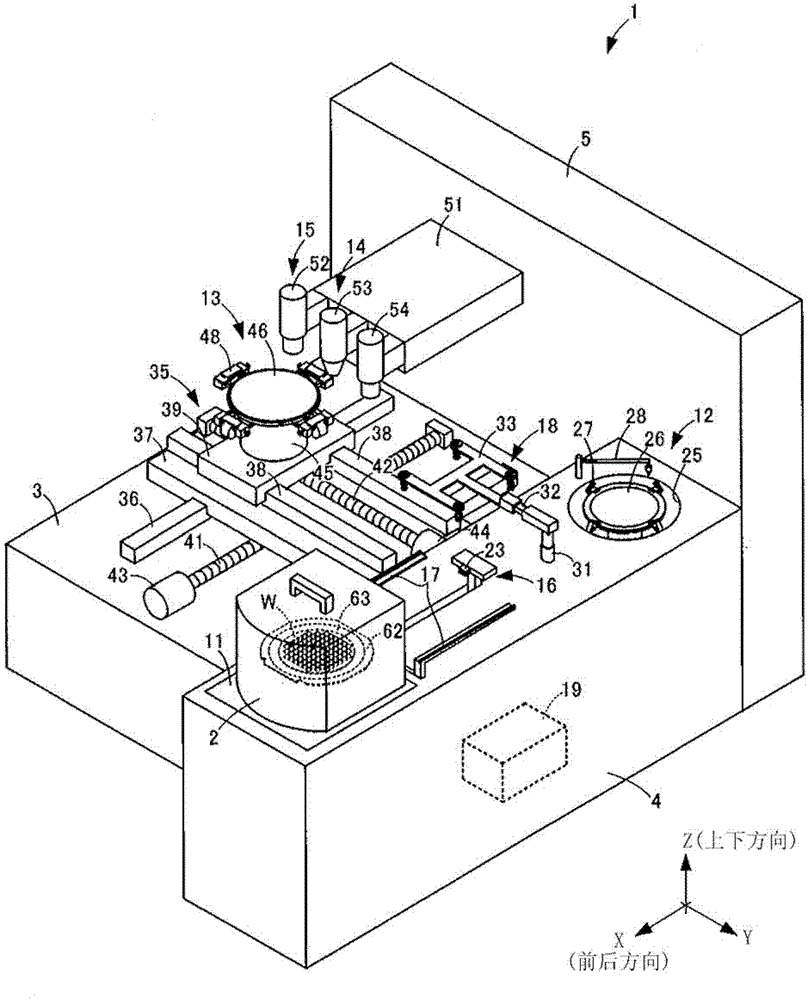
[0040] refer to figure 1 , the laser processing apparatus to which the measurement method according to the present invention is applied will be described. figure 1 It is a perspective view of the laser processing apparatus according to the embodiment of the present invention. In addition, the laser processing device to which the measurement method of the present invention is applied is not limited to figure 1 structure shown. The laser processing device may have any structure as long as it is a structure for performing laser processing on a workpiece. In addition, the assay method of the present invention is not limited to be applicable to figure 1 The configuration of the laser processing apparatus shown above can be applied, for example, to a measurement apparatus dedicated to film thickness measurement that is different from the laser processing apparatus.

[0041] Such as figure 1 As shown, the laser processing device 1 is configured as a protective film 61 for preven...


PUM


Abstract

PROBLEM TO BE SOLVED: To provide a measuring method and a measuring apparatus capable of accurately measuring a thickness of a protective film formed on a workpiece surface.SOLUTION: The measuring method of the invention comprises: a step of forming a protective film 61 containing a light absorption agent on a wafer W; a step of irradiating the wafer W with a measuring beam via the protective film 61 and receiving a reflected light from the wafer W; and a step of referencing measurement data indicating change of the reflection intensity of the wafer W for change of the thickness of the protective film 61 manufactured in advance and measuring the thickness of the protective film 61 from the reflection intensity of the wafer W.

Description

technical field [0001] The present invention relates to a measuring method and a measuring device for measuring the thickness of a protective film formed on the surface of a workpiece. Background technique [0002] As a method of dividing workpieces such as semiconductor wafers along dicing lines, a method of dividing by laser processing is known (for example, refer to Patent Document 1). In the laser processing method of Patent Document 1, the semiconductor wafer is continuously processed along the dicing line by irradiating laser beams to the semiconductor wafer and thermal energy generated in the irradiated region. In the irradiated area on the semiconductor wafer, thermal energy may be concentrated to generate chips (processing chips). There is a problem that the chips adhere to the bonding pads of the LSI, etc., thereby degrading the quality of the semiconductor chip. [0003] In order to solve this problem, the present applicant has developed a laser processing method...

Claims


Application Information

Patent Timeline
Patent Type & Authority Patents(China)
IPC IPC(8): G01B11/06B23K26/00B23K26/18
CPCG01B9/0209G01B11/0616G01N21/55G01N21/8483G01N21/9501H01L22/00
Inventor 北原信康高桥邦充大浦幸伸
Owner DISCO CORP
Why Eureka
Try Eureka