
Ultra-thin silicon PIN high energy particle detector based on bonding substrate and manufacturing method thereof

A high-energy particle and detector technology, applied in semiconductor devices, final product manufacturing, sustainable manufacturing/processing, etc., can solve the problems of increased corrosion time, increased leakage current, uncontrollable detector thickness, etc., to reduce detection The effect of detector leakage current, detector thickness determination, and detector thickness controllable

Inactive Publication Date: 2014-04-16
PEKING UNIV
View PDF2 Cites 0 Cited by
  • Summary
  • Abstract
  • Description
  • Claims
  • Application Information

AI Technical Summary

Problems solved by technology

[0005] However, using TMAH to etch the silicon substrate to thin it will also bring many problems
First of all, this method obtains the detector with the required thickness by controlling the corrosion time and the corrosion rate under the corresponding corrosion conditions, but the corrosion rate is affected by many factors, and it is impossible to obtain a completely definite and constant corrosion rate, which leads to The thickness of the detector is uncontrollable, uneven, and not repeatable, which is a fatal problem for production applications, because, for the application of ΔE ultra-thin detectors, the identification of particles is directly related to the thickness of the ΔE detector, and the thickness is inconsistent It means that each detector must be equipped with a corresponding processing system, which cannot be used in batches
Secondly, wet etching will inevitably increase the roughness of the detector surface, resulting in an increase in leakage current, thereby affecting the resolution of the detector, although this can be achieved by slowing down the corrosion rate to obtain a relatively rough corrosion surface. Controlling the leakage current improves the detector resolution, but it cannot fundamentally eliminate this defect, and it also increases the corrosion time, which is not good for production applications
The above problems make it impossible for us to mass-produce high-performance detectors with a certain thickness and the same thickness

Method used


Image

  • Ultra-thin silicon PIN high energy particle detector based on bonding substrate and manufacturing method thereof
  • Ultra-thin silicon PIN high energy particle detector based on bonding substrate and manufacturing method thereof
  • Ultra-thin silicon PIN high energy particle detector based on bonding substrate and manufacturing method thereof

Examples


Embodiment Construction

[0052] The bonded substrate ultra-thin silicon PIN high-energy particle detector and its preparation method of the present invention will be further described in detail below in conjunction with the best examples shown in the accompanying drawings.

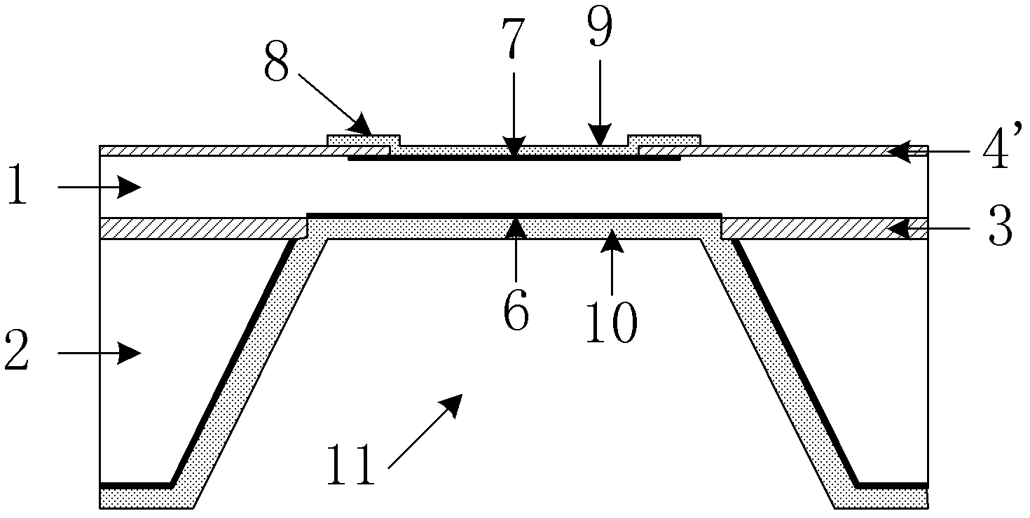
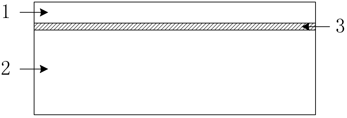
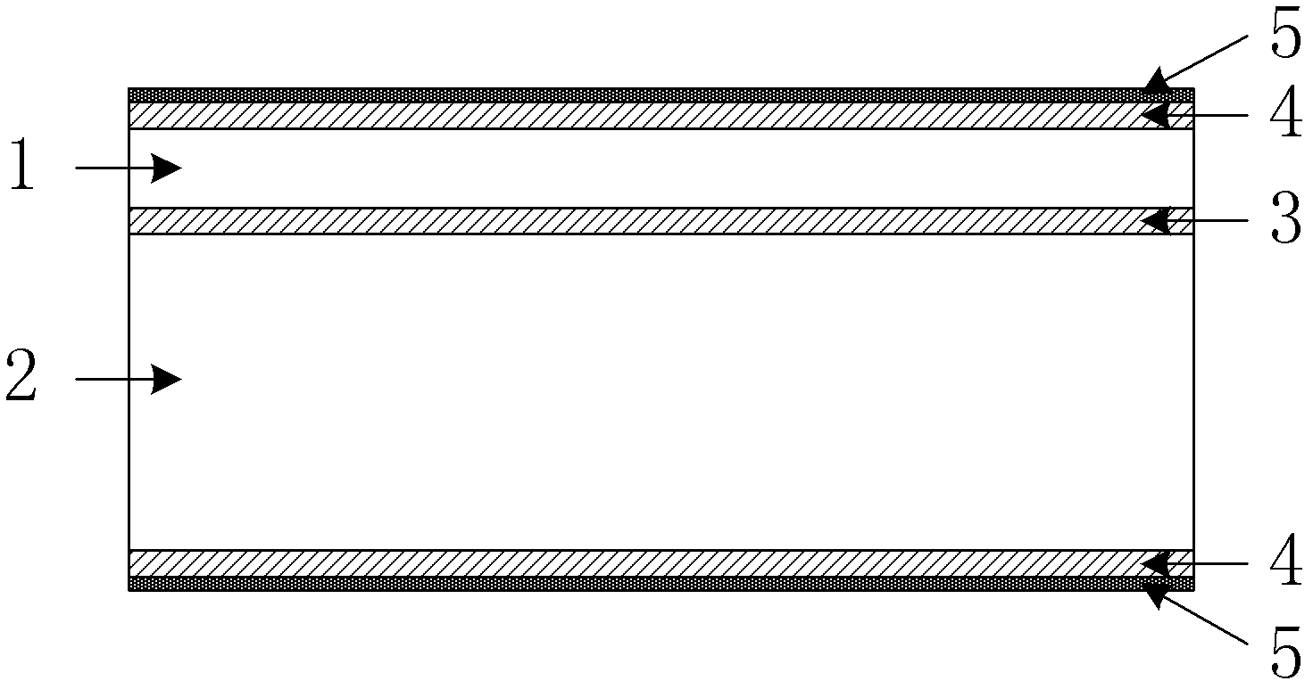
[0053] Such as figure 1 As shown, the ultra-thin silicon PIN high-energy particle detector structure based on the bonded substrate includes: a bonded silicon substrate composed of a device layer silicon chip 1 and a supporting layer silicon chip 2, wherein the device layer silicon chip 1 is a (111) crystal Oriented N-type silicon with a resistivity greater than 4000 ohm·cm and a thickness of 100 μm; the supporting layer silicon wafer 2 is (100) oriented N-type silicon with a resistivity of 2-4 ohm·cm and a thickness of 400 μm.

[0054] The front side of the device layer silicon wafer 1 has a boron-doped P + Region 7, to form PN junction, has thin aluminum layer 9 to cover on it, and thin aluminum layer 9 has field plate structure...


PUM


Abstract

The invention discloses an ultra-thin silicon PIN high energy particle detector based on a bonding substrate and a manufacturing method thereof. The detector comprises: a device layer silicon chip, a support layer silicon chip and a silicon dioxide layer, wherein the device layer silicon chip and the support layer silicon chip are bonded together; the silicon dioxide layer is arranged between the device layer silicon chip and the support layer silicon chip. A right side of the device layer silicon chip is provided with a P<+> area which is formed by doping. A silicon surface, except of the P<+> area, is covered by the silicon dioxide layer. The P<+> area is covered by a thin metal layer. An edge of the thin metal layer possesses a field board structure. The support layer silicon chip is provided with a window on a position corresponding to the device layer silicon chip P<+> area so as to form a cavity structure which exposes a back side of the device layer silicon chip. The cavity structure is in an upturned barrel shape which is wide on the bottom and narrow on above part. The back side area exposed by the device layer silicon chip is N<+> area which is formed by doping. The N<+> area surface is covered by a thick metal layer. The ultra-thin detector of the invention can measure particle energy and identify particle kinds. The detector can be applied in nuclear physics detection field and the like.

Description

technical field [0001] The invention relates to an ultra-thin silicon PIN high-energy particle detector, in particular to an ultra-thin silicon PIN high-energy particle detector based on a bonded substrate and a preparation method thereof, which is the first among ΔE-E telescopes applicable to nuclear radiation detection applications. Layer ΔE ultrathin detectors. Background technique [0002] The silicon PIN detector measures the particle energy and identifies the particle type by detecting the instantaneous pulse current signal generated by the radiation particles entering the detector. Silicon PIN detectors have the characteristics of simple structure, high sensitivity, good linear response, fast time response, large dynamic range, strong anti-radiation performance, and stable vacuum performance. They are important in nuclear physics research such as measurement and diagnosis of pulsed radiation fields. Value. [0003] Ultra-thin silicon PIN high-energy particle detecto...

Claims


Application Information

Patent Timeline
Patent Type & Authority Patents(China)
IPC IPC(8): H01L31/0203H01L31/105H01L31/18
CPCY02P70/50
Inventor 于民董显山田大宇金玉丰
Owner PEKING UNIV
Learn More