Method for forming microscopic structures on a substrate

A microstructure and substrate technology, applied in the direction of microstructure devices, manufacturing microstructure devices, microstructure technology, etc., can solve problems such as the use of photolithography technology and the limitation of the minimum feature size of patterned structures

Active Publication Date: 2015-01-28
FEI CO
View PDF5 Cites 0 Cited by
  • Summary
  • Abstract
  • Description
  • Claims
  • Application Information

AI Technical Summary

Problems solved by technology

[0004] A disadvantage of the described method is that the minimum feature size of the patterned structure is limited by the photolithographic process and subsequent etching
[0005] Another disadvantage of the described method is the use of a photolithographic process and the large number of steps it implies

Method used


Image

  • Method for forming microscopic structures on a substrate
  • Method for forming microscopic structures on a substrate
  • Method for forming microscopic structures on a substrate

Examples


Embodiment Construction

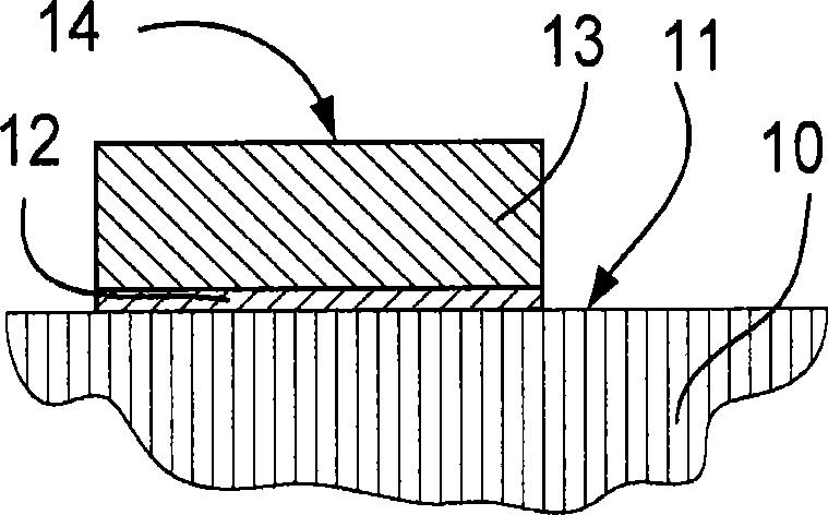
[0041] Figure 1A schematically shows a cross-section of a substrate with microstructures thereon, while Figure 1B The same substrate is shown viewed from the side where the microstructures were grown on the substrate.

[0042] Figure 1A and 1B A substrate 10 is shown having a surface 11 on which a seed layer 12 is deposited using EBID or IBID. The seed layer is then thickened with a material 13 showing a surface 14 substantially parallel to the substrate surface using eg ALD or CVD. The substrate 10 may be a semiconductor substrate, such as a wafer or chip, showing a surface of, for example, silicon oxide, silicon nitride, or aluminum oxide. However, other materials can also be used as the substrate, such as diamond or any other material on which the seed layer can be deposited.

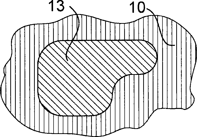
[0043] figure 2 A substrate on which a seed layer is formed is schematically illustrated.

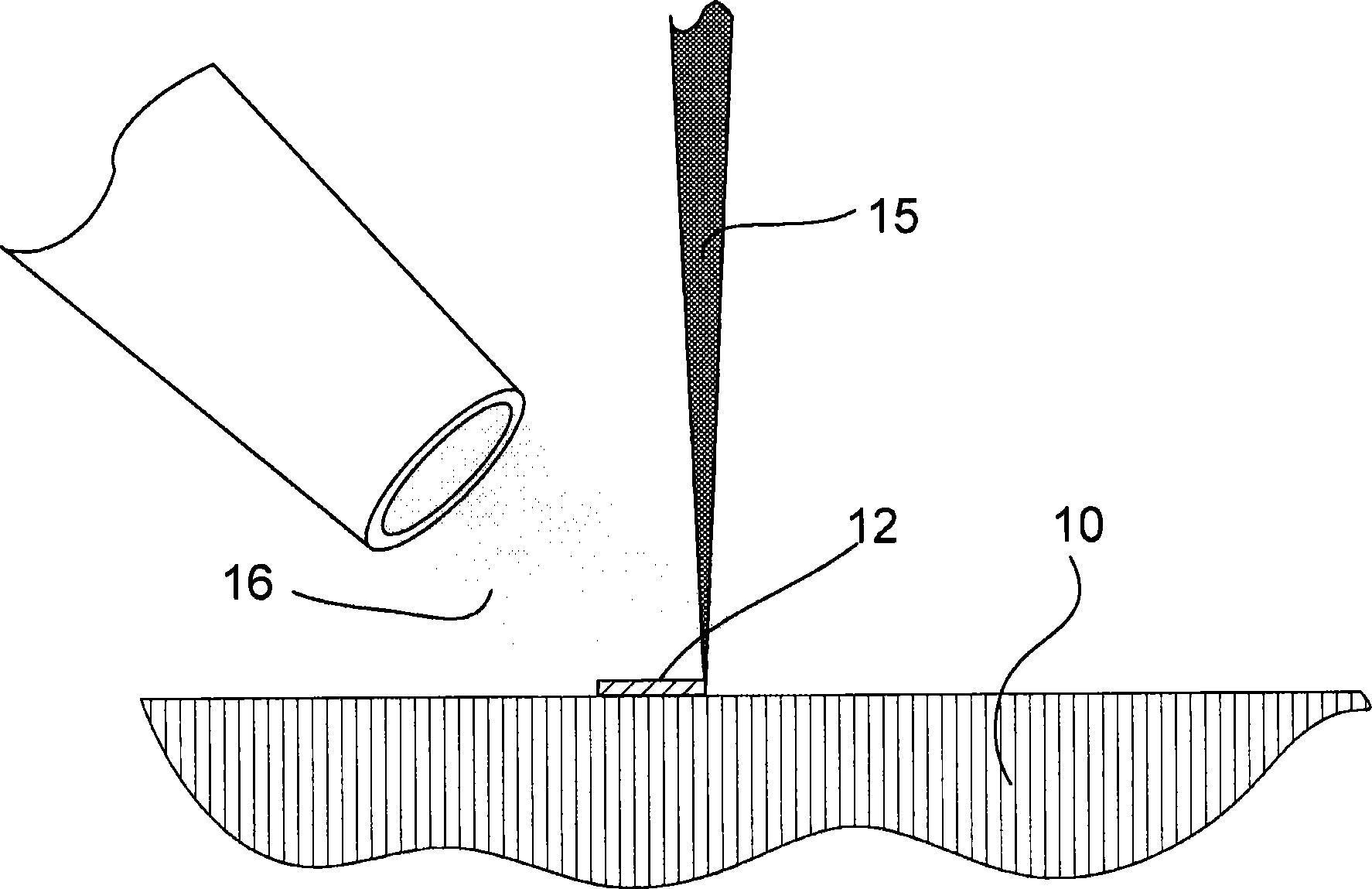
[0044] figure 2 A substrate 10 is shown on which a focused particle beam 15 , such as an electro...


PUM


Abstract

The invention relates to a method for forming microscopic structures. By scanning a focused particle beam over a substrate in the presence of a precursor fluid, a patterned seed layer is formed. By now growing this layer with Atomic Layer Deposition or Chemical Vapour Deposition, a high quality layer can be grown. An advantage of this method is that forming the seed layer takes relatively little time, as only a very thin layer needs to be deposited.

Description

technical field [0001] The present invention relates to a method for forming a microstructure on a substrate, the method comprising: providing a substrate having a surface on which a patterned seed layer having a desired shape is formed , and thickening the patterned seed layer in such a manner as to form a structure having a surface substantially parallel to the surface of the substrate. Background technique [0002] This method is described in "Low-temperatureatomic-layer-deposition lift-off method for microelectronic and nanoelectronic applications" by M.J.Biercuk et al. (Appl.Phys.Lett., Vol.83, No.12, Sept.2003, pp.2405-2407 , DOI: 10.1063 / 1.612904) is published. [0003] The foregoing methods disclose growing a patterned dielectric film on a substrate. The substrate was a polished silicon wafer with a 1 μm thick thermally grown oxide layer. A resist layer was spin-coated on the substrate. The pattern is formed in the resist by photolithographic techniques or direct...

Claims


Application Information

Patent Timeline
Patent Type & Authority Patents(China)
IPC IPC(8): B81C1/00
CPCC30B25/02C23C16/18C23C16/047C30B23/02
Inventor A·F·德琼格J·J·L·穆尔德斯A·J·M·麦克库斯W·M·M·克塞尔斯
Owner FEI CO
Why Eureka
Try Eureka