Method for detecting critical cutting depth of hard and brittle ceramic material
A critical cutting depth, ceramic material technology, used in measuring devices, instruments, optical devices, etc., can solve the problems of poor reliability and poor detection accuracy, and achieve the effect of consistent processing conditions, high accuracy and high resolution
- Summary
- Abstract
- Description
- Claims
- Application Information
AI Technical Summary
Problems solved by technology
Method used
Image
Examples
example 1
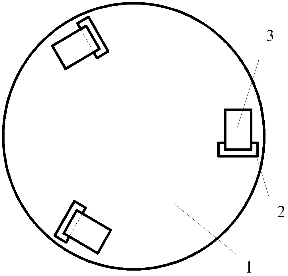
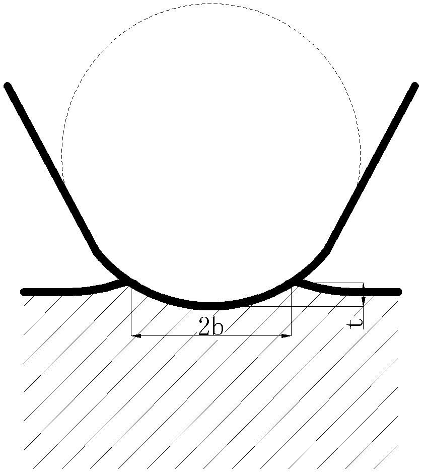
[0026] Example 1: The critical cutting depth of single crystal silicon is not only related to its own material properties, but also many other influencing factors. Among them, the cutting depth of plastic-brittle transition of cuts with different widths is different. Generally, wide cuts are prone to brittle fracture, and narrow cuts are prone to plastic cutting. It is generally believed that the width of cuts is determined by the size of abrasive grains. However, in the inspection of the processing area, it will be found that some wide cut marks are still plastic cutting when the cutting depth is deep, and some narrow cut marks appear brittle fracture when the cutting depth is shallow. Therefore, the cutting must be considered comprehensively. The width and depth of the mark. Since the shape of the cut mark of the workpiece is formed by cutting with a round edge, the radius of the round edge of the abrasive particle tip takes into account the width and depth of the cut mark, s...
example 2
[0031] Example 2: The main crystal planes of single crystal silicon are {100}, {110} and {111}, and their interplanar spacing, areal density and bond density are all different, so single crystal silicon crystal has the characteristics of anisotropy. The {111} crystal planes have the largest atomic density and the highest elastic modulus, but the interplanar spacing is large, and the atomic bond density on the planes is low, and the {111} crystal planes are relatively fragile. The elastic modulus and atomic bonds of the {110} crystal plane are second only to the {111} crystal plane. {100} The crystal plane spacing is the smallest and the bond density is the largest. Therefore, single crystal silicon crystals are most likely to be cleaved along the {111} crystal plane at room temperature, and the {111} crystal plane is the second cleavage plane. At present, the most commonly used in the semiconductor industry are single crystal silicon wafers with {100} crystal faces and {111} c...
PUM
 Abstract
Description
Claims
Application Information


