

Method for enlarging bonding area of chip
A chip bonding and area technology, applied in the direction of sustainable manufacturing/processing, electrical components, climate sustainability, etc., can solve problems such as poor appearance, grain loss, and increased manufacturing costs, so as to save chemicals and equipment use The effect of reducing the abnormal occurrence of bonded layer shedding, and the operation of the equipment is simple and convenient
Inactive Publication Date: 2012-07-11
BEIJING TIMES HAODING TECH
View PDF3 Cites 0 Cited by
- Summary
- Abstract
- Description
- Claims
- Application Information
AI Technical Summary
Problems solved by technology
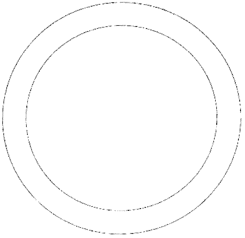
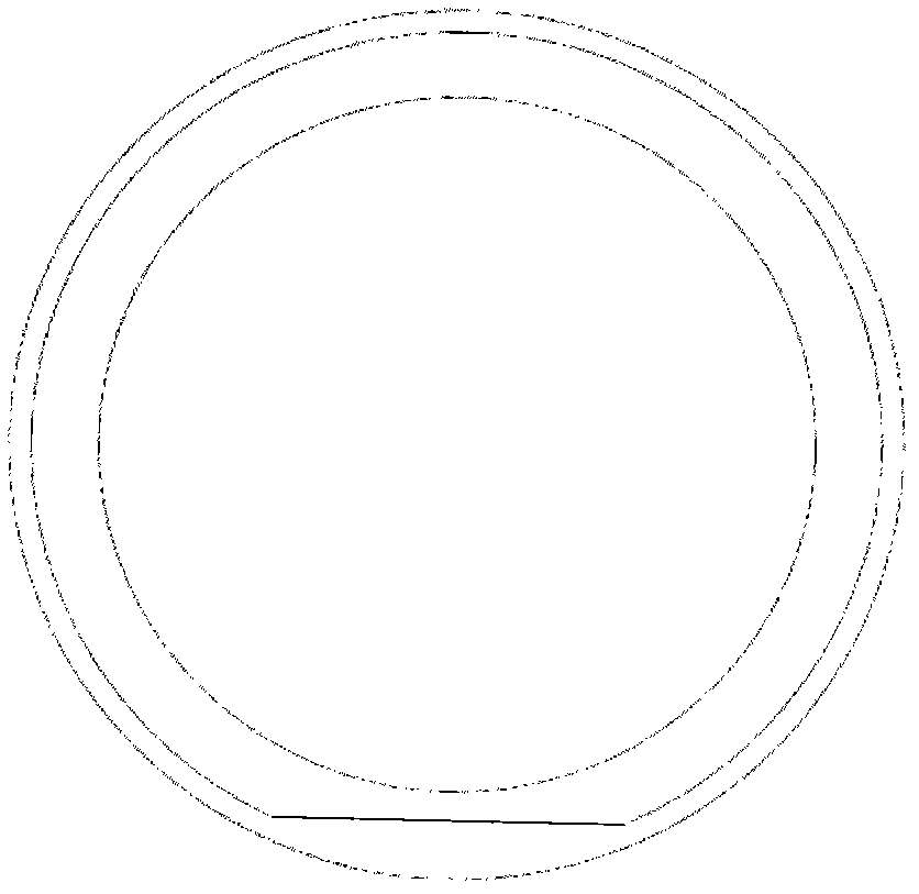
At present, in the existing chip bonding process, a back-mounted plating pot is used when the chip is evaporated (such as figure 2 shown), the edge is due to the evaporation cover ( image 3 ) ring, the evaporated material cannot be deposited on the edge of the wafer, resulting in a small bonding area, voids in the bonding area, and interlayers. Lamination peeling off, high voltage, poor appearance and other abnormalities, resulting in a large loss of grains, low yield, and increased manufacturing costs
Method used
View moreImage
Smart ImageViewing Examples

Examples
Embodiment Construction
[0016] The present invention can adopt following implementation method to realize:
[0017] (1) the wafer is cleaned;
[0018] (2) Put the vapor deposition target in the coating machine, then place the wafer in the vertical plating pot, and put the plating pot into the coating machine;
[0019] (3) Vacuuming 4.5×10 -4 Pa, began to evaporate.
[0020] (4) After the evaporation is completed, the wafer is removed from the positive plating pot for bonding.
Login to View More PUM
 Abstract
The invention provides a method for enlarging a bonding area of a chip. The method comprises the following steps of: placing a wafer to be bonded on a wafer gasket by utilizing a front-placed evaporation boiler; fixing the wafer gasket by a spring clip to carry out evaporation or deposition on a bonding material and then placing the wafer with the evaporated bonding material into a bonding machine to carry out bonding work; and bonding the wafer / the wafer or the wafer / a silicon sheet together. By utilizing the method to bond the wafer / the wafer or the wafer / the silicon sheet, the bonding area of a bonded substrate sheet is higher than 99.99%, the bonding material does not overflow and no cavity is generated, high bonding strength is achieved, and the bonding rate is higher than 99%; and the prepared substrate sheet has no polluted layers, polycrystalline layers and oxidized layers in a bonding region, the yield of a subsequent process is improved and the production cost is reduced. Therefore, the performance of a manufactured diode light-emitting device is greatly improved and an LED (Light-Emitting Diode) device with high efficiency, high brightness, low resistance and stable performance can be prepared.
Description
technical field [0001] The invention patent relates to a method for increasing the chip bonding area Background technique [0002] The semiconductor lighting industry has risen in the world. In the national medium and long-term science and technology planning strategy seminar, the "New Century Lighting Project" has been recommended as a major project, and the development of semiconductor lighting projects has entered a new era. Chip bonding technology is an important technology in the field of semiconductor optoelectronics and power electronics. It adds some kind of adhesive between two chips, and then bonds them together by chemical or physical methods to form a new substrate. At present, in the existing chip bonding process, a back-mounted plating pot is used when the chip is evaporated (such as figure 2 shown), the edge is due to the evaporation cover ( image 3 ) ring, the evaporated material cannot be deposited on the edge of the wafer, resulting in a small bonding ar...
Claims
Login to View More Application Information
Patent Timeline
 Patent Type & AuthorityApplications(China)
IPC IPC(8): H01L21/60
CPCY02P70/50
Inventor杨继远
OwnerBEIJING TIMES HAODING TECH