

Multilayer spacer type IC (Integrated Circuit) chip stacked package of substrate and production method of package
A chip stacking and production method technology, applied in the direction of electrical components, semiconductor devices, electrical solid devices, etc., can solve problems such as poor insulation performance, affecting chip heat dissipation, and affecting the height of bonding wires connecting IC chips and carrier pads, etc. , to achieve the effect of facilitating heat dissipation, improving insulation performance and solving height problems
- Summary
- Abstract
- Description
- Claims
- Application Information
AI Technical Summary
Problems solved by technology
Method used
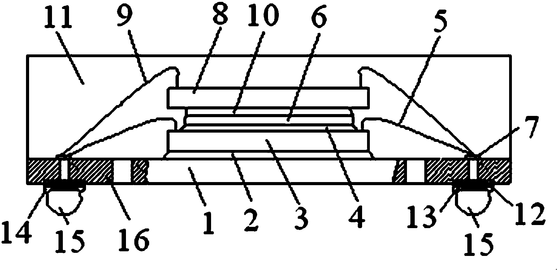
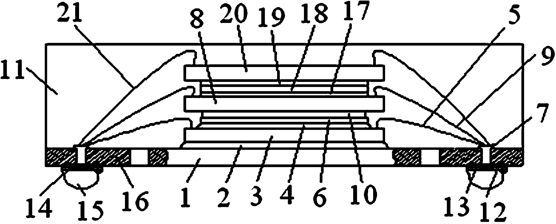
Image

Examples
Embodiment 1
[0104] The chip thickness is reduced from the original wafer thickness to the final thickness of 100μm; the rough grinding range is from the original wafer thickness to 150μm + film thickness, and the rough grinding speed is 2μm / s; the fine grinding thickness ranges from 150μm + film thickness to 100μm + Film thickness, fine grinding speed 0.6μm / s, chip warping prevention process is used during wafer thinning; the roughness of thinned wafer is 0.10mm, using DISC 3350 dicing machine to dicing, using anti-fragmentation , Anti-crack dicing process software control technology, dicing feed speed ≤10mm / s; get separated IC chip with bandage ring; thin the single wafer to make the final thickness 110μm; during the thinning process of single wafer, rough grinding Range from the original thickness of single wafer to 160μm + film thickness, rough grinding speed 3μm / s; fine grinding thickness range from 160μm + film thickness to 110μm + film thickness, fine grinding speed 15μm / s; core is a...
Embodiment 2
[0106] The chip thickness is reduced from the original wafer thickness to the final thickness of 100μm; the rough grinding range is from the original wafer thickness to 150μm + film thickness, and the rough grinding speed is 5μm / s; the fine grinding thickness ranges from 150μm + film thickness to 100μm +Adhesive film thickness, fine grinding speed 0.3μm / s, chip warping prevention process is used during wafer thinning; the roughness of the thinned wafer is 0.05mm; double knife dicing machine is used for dicing, and anti- Chip and anti-crack scribing process software control technology, scribing feed speed ≤10mm / s; get separated IC chip with bandage ring. Thin the single wafer to a final thickness of 120μm; during the process of single wafer thinning, the rough grinding range is from the original thickness of the single wafer to 170μm + film thickness, and the rough grinding speed is 5μm / s; the fine grinding thickness ranges from 170μm + film thickness To 120μm + film thickness, ...
Embodiment 3
[0108] The chip thickness is reduced from the original wafer thickness to the final thickness of 100μm; the rough grinding range is from the original wafer thickness to 150μm + film thickness, and the rough grinding speed is 3.5μm / s; the fine grinding thickness ranges from 150μm + film thickness to 100μm + film thickness, fine grinding speed 0.45μm / s, chip warping prevention process is used in the process of wafer thinning; the roughness of the thinned wafer is 0.08mm, using A-WD-3000TXB dicing machine Chips; using anti-fragment and anti-crack dicing technology software control technology, dicing feed speed ≤10mm / s; get separated IC chip with bandage ring; thin the single chip to make the final thickness of 100μm; single chip thinning In the process, the rough grinding range is from the original thickness of the single wafer to 150μm + film thickness, and the rough grinding speed is 4μm / s; the fine grinding thickness ranges from 150μm + film thickness to 100μm + film thickness, ...
PUM
 Abstract
Description
Claims
Application Information