Solar cell capable of saving silver paste and preparation process thereof
A technology for solar cells and silver paste, applied in the field of solar cells, can solve the problems of high cost and complex preparation process, and achieve the effects of high production efficiency, good electrical conductivity, and reduction of welding equipment and personnel investment.
- Summary
- Abstract
- Description
- Claims
- Application Information
AI Technical Summary
Problems solved by technology
Method used
Image
Examples
Embodiment 1
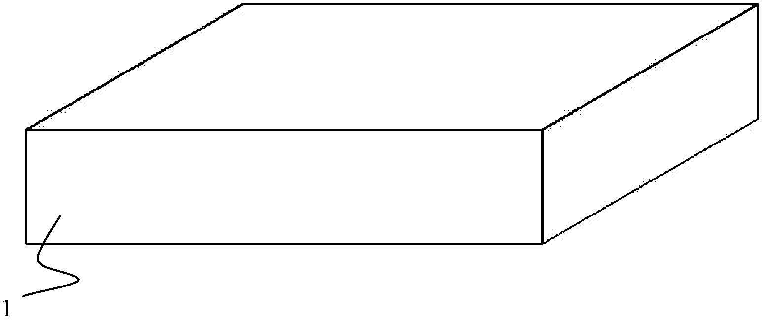
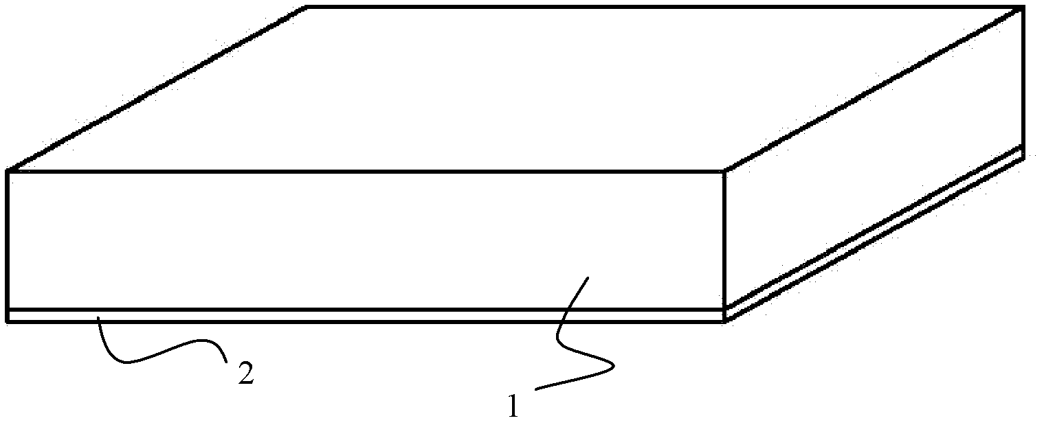
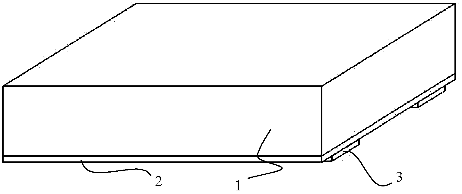
[0041] Such as Figure 1 to Figure 7 As shown, a solar cell that can save silver paste according to the present invention includes a silicon wafer 1, the back of the silicon wafer 1 is printed with an all-aluminum paste layer 2, and the back of the silicon wafer 1 is printed with an all-aluminum paste layer 2 is provided with a silver-plated copper strip 3 on the back, and the front of the silicon chip 1 is provided with a pattern of auxiliary grid lines 4, and the surface of the auxiliary grid lines 4 is provided with a number of silver-plated front surfaces with silver paste 5 on the bottom surface. Copper strips 6, the front silver-plated copper strips 6 are arranged at intervals and extend outward from the side of the silicon chip 1 and toward the back of the adjacent silicon chip. The main grid line 61 of the electrode and the soldering strip 62 that bends and extends outward and toward the back of the silicon chip 1, and the soldering material 62 is provided on the solde...
Embodiment 2
[0052] This embodiment is basically the same as the above-mentioned embodiment 1, the difference is that the specific steps of the solar cell preparation process are different: specifically, the thickness of the aluminum paste layer 2 in the above step (1) is 15-20 μm;
[0053] In the above step (2), the width of the silver-plated copper strip 3 on the back is 2mm, and the silver-plated thickness on the silver-plated copper strip 3 on the back is 1 μm, and its surface roughness is R6.4;
[0054] In the above step (3), the width of the auxiliary gate line 4 is 90 μm, and the height is 15-20 μm;
[0055] In the above step (4), the thickness of the silver paste 5 is 15-20 μm, and the front silver-plated copper strip 6 directly above the front of the silicon wafer 1 has a width of 600 μm and a height of 300 μm; The width of the epitaxial part is 1.2 mm, the height is 200 μm, the silver plating thickness on the front silver-plated copper strip 6 is 1 μm, and its surface roughness i...
Embodiment 3
[0058] This embodiment is basically the same as the preceding two embodiments, and the difference is that in the preparation process:
[0059] The thickness of the aluminum paste layer 2 in the above step (1) is 20-25 μm;
[0060] The width of the silver-plated copper strip 3 on the back side in the above step (2) is 2.5 mm, the silver-plated thickness on it is 2 μm, and the surface roughness is R12.5;
[0061] In the above step (3), the auxiliary gate line 4 has a width of 100 μm and a height of 25-30 μm;
[0062] The front silver-plated copper strip 6 that is brushed with silver paste 5 on the bottom surface of the above-mentioned steps (4) is pressed on the above-mentioned silicon chip 1 front with the auxiliary grid line 4 pattern, and is dried by a drying furnace. The thickness of the silver paste 5 is 25-30 μm, the width of busbar 61 in the front silver-plated copper strip 6 directly above the front surface of silicon wafer 1 is 900 μm, and the height is 250 μm, and the...
PUM
| Property | Measurement | Unit |
|---|---|---|
| Resistivity | aaaaa | aaaaa |
| Thickness | aaaaa | aaaaa |
| Thickness | aaaaa | aaaaa |
Abstract
Description
Claims
Application Information


