InAs/GaSb secondary category superlattice infrared detector

A technology of infrared detector and superlattice, which is applied in the direction of semiconductor devices, electrical components, circuits, etc., can solve the problem that the bandgap width is not large enough

Inactive Publication Date: 2012-07-11
INST OF SEMICONDUCTORS - CHINESE ACAD OF SCI
View PDF1 Cites 32 Cited by
  • Summary
  • Abstract
  • Description
  • Claims
  • Application Information

AI Technical Summary

Problems solved by technology

Its disadvantage is that it is easy to generate surface states of dangling bonds on the

Method used


Image

  • InAs/GaSb secondary category superlattice infrared detector
  • InAs/GaSb secondary category superlattice infrared detector
  • InAs/GaSb secondary category superlattice infrared detector

Examples


Embodiment Construction

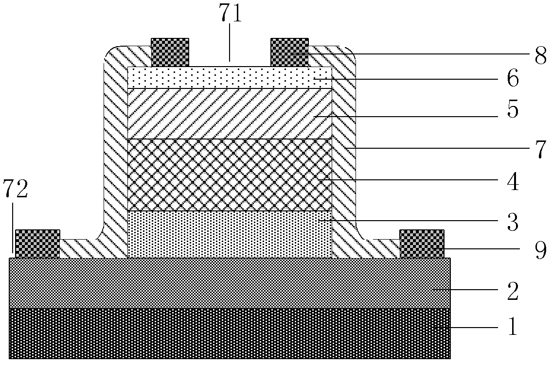
[0025] see figure 1 As shown, the present invention provides a kind of InAs / GaSb class II superlattice infrared detector, comprising:

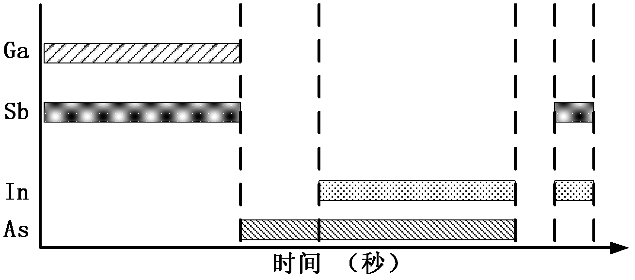
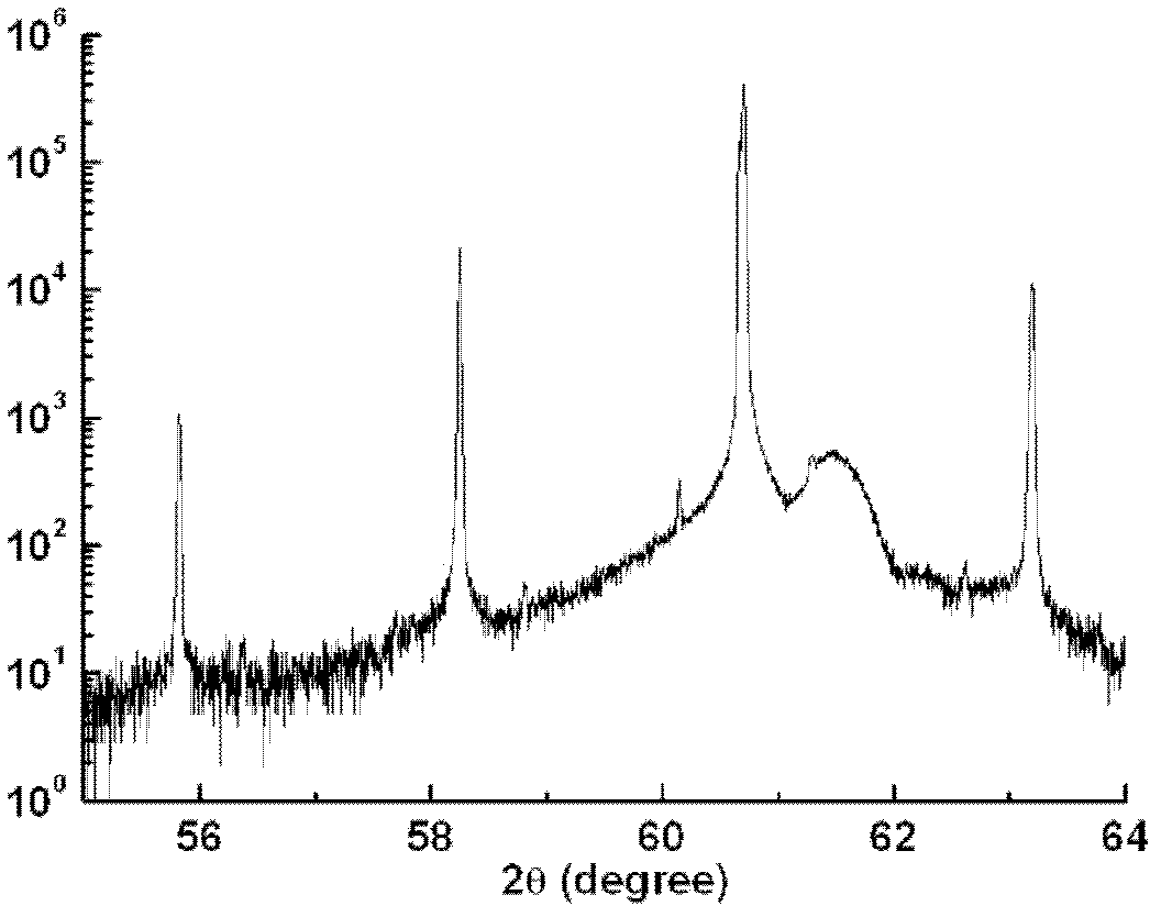
[0026] A substrate 1, the material of the substrate 1 is GaSb; before making the InAs / GaSb type II superlattice infrared detector on the substrate 1, the GaSb substrate 1 is placed in the buffer chamber of the molecular beam epitaxy equipment system The degassing table is degassed, the degassing time is 40 minutes to 2 hours, and the degassing temperature is 180 to 240 ° C; the purpose of degassing is to remove the water vapor on the surface of the GaSb substrate 1 and prevent it from being brought into the growth chamber; then Put the GaSb substrate 1 into the growth chamber of the molecular beam epitaxy equipment system, place it in the growth position, deoxidize at 525°C, raise the temperature of the GaSb substrate 1 to 545°C and protect it under the Sb atmosphere for 5 to 10 minutes. The purpose is to remove oxides on the surface of the G...


PUM

PropertyMeasurementUnit
Thicknessaaaaaaaaaa
Thicknessaaaaaaaaaa
Thicknessaaaaaaaaaa

Abstract

The invention relates to an InAs/GaSb secondary category superlattice infrared detector. The infrared detector comprises: a substrate; a buffer ohmic contact layer, which is manufactured on the substrate; a first secondary category superlattice layer, which is manufactured on the buffer ohmic contact layer so as to enable table tops to be formed at two sides above the buffer ohmic contact layer; an intrinsic secondary category superlattice light absorption layer, which is manufactured on the first secondary category superlattice layer; a second secondary category superlattice layer, which is manufactured on the intrinsic secondary category superlattice light absorption layer; an ohmic contact layer, which is manufactured on the second secondary category superlattice layer; a passivation layer, which covers portions of the table tops at the two sides of the buffer ohmic contact layer, side surfaces of the first secondary category superlattice layer, the intrinsic secondary category superlattice light absorption layer, the second secondary category superlattice layer and the ohmic contact layer as well as two side surfaces on the ohmic contact layer; upper electrodes, which are manufactured at two sides of a light transmission opening; and lower electrodes, which are manufactured inside electrode windows. Specifically, the light transmission opening is arranged in the middle of the passivation layer covering the ohmic contact layer; and the electrode windows are respectively arranged on the two table tops at two sides of the passivation layer covering the buffer ohmic contact layer.

Description

technical field [0001] The invention relates to the technical field of using semiconductors, in particular to a method for making and passivating an InAs / GaSb type II superlattice infrared detector in the 3 to 5 micron medium wave band. Background technique [0002] Since the first practical infrared detector was successfully developed in the 1940s, infrared detectors have been widely used in many fields such as civil, military, and space. Infrared systems composed of infrared detectors have been widely used in night vision, navigation, search, early warning, target reconnaissance, precision strikes, etc. Strong interference and other advantages. For the InAs / GaSb type II superlattice infrared detector, because in the InAs / GaSb type II superlattice, electrons are mainly bound in the InAs layer, while holes are mainly bound in the GaSb layer, so electrons and holes form Space isolation has the following advantages: [0003] 1) High quantum efficiency, inter-band transition...

Claims


Application Information

Patent Timeline
IPC IPC(8): H01L31/101H01L31/0352H01L31/0304
Inventor 黄建亮马文全张艳华曹玉莲
Owner INST OF SEMICONDUCTORS - CHINESE ACAD OF SCI
Why Eureka
Try Eureka